FPGA Accelerated RF Wideband Measurements
with Guzik ADC6000 8-bit FPGA-based Digitizers
- FPGA-accelerated digital slice-equalization to improve SFDR
- FPGA-accelerated Digital Down Conversion DDC (up-to 13 GHz) with post-memory IF Magnitude triggering
- FPGA-based Real-Time 10 Gsa/s FPGA-based DDC (up-to 4 GHz)
- With Real-Time IF Magnitude triggering and Variable Length Segmented Acquisition
- FPGA-accelerated Digital Filtering and Decimation to increase ADC resolution, reduce data speed and decrease offloading time for Baseband and (I+jQ) measurements
- FPGA-based periodic real-time averaging (single segment and multi-segmented)
- Up-to 128 GByte of memory on board. (64 GByte standard)
- Segmented acquisitions with reduced inter-segment dead time.
- PCIe Gen2 x4 and AXIe backplane real-time streaming interface for offloading data
- Multichannel scalable coherent acquisition in AXIe modular form factor
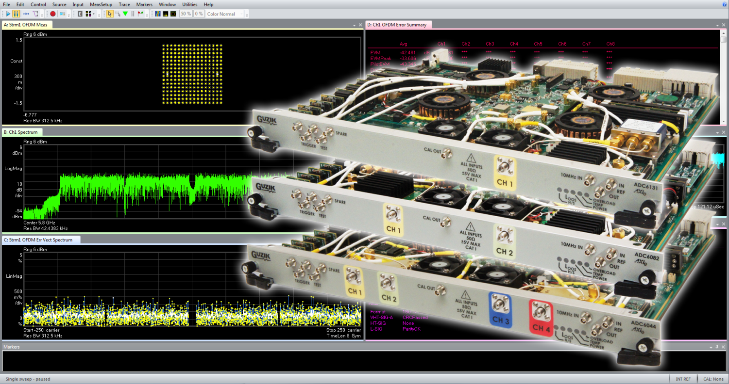
Solutions for
Hardware Accelerated and Real-Time RF Wideband Digital Communications and Aerospace & Defense Measurements
Using wide bandwidth digitizers to directly acquire, down convert, process Digital Communications, Wireless, Radar and Satcom standards up to 13 GHz and analyze with the Keysight 89600 VSA Software.
Introduction
High speed digitizers are becoming popular for Vector Signal Analysis (VSA) and baseband measurements because well-known advantages of digital processing: repeatability, stability and flexibility of digital measurements.
There are two possibilities for this type of measurements: perform digital down conversion (DDC) in PC or implement it in hardware which is part of a digitizer. The second approach has critical advantages because it reduces the amount of data transferred to PC and in return significantly increases measurement speeds for UPH testing.
Product description
The ADC6000 Series 8-bit AXIe Waveform Digitizers offer 3 models with wide tunable operating analog input range from -24 dBm to + 22 dBm, providing either ADC6044 4 channels of 10 Gsa/s sampling with 4 GHz bandwidth, ADC6082 2 channels of 20 Gsa/s sampling with 8 GHz bandwidth, or ADC6131 1 channel of 40 Gsa/s sampling with 13 GHz bandwidth, each with 8-bit vertical resolution, in a single-slot AXIe format. This selection makes these models ideal for low to high channel density system integrations.
- 1 channel, DC to 13 GHz bandwidth*, 40 Gsa/s
- 2 channels, DC to 8 GHz bandwidth*, 20 Gsa/s
- 4 channels, DC to 4 GHz bandwidth*, 10 Gsa/s
(Supports 2 channels, DC to 6.5 GHz bandwidth*, 20 Gsa/s mode)
*Analog Bandwidth (-3db)1,2
________________
1 With digital equalization.
2 6-pole Butterworth approximation.
Block diagram
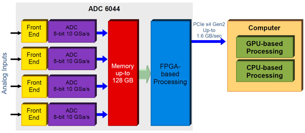
Figure 1 Simplified block diagram of the ADC6044 in a standard Keysight AXIe chassis
Digitizers with DDC Accelerated
In the digitizers the accelerated DDC is implemented using FPGAs (Figure 1). The data from ADC is transferred to the memory and from memory through digital equalizer to DDC. The down conversion is implemented by two multipliers with Sin/Cos LO signals. Down converted signals connected through LPF/decimator to I/Q memory and transferred to PC. Analysis software like Keysight VSA 89600 software performs final processing and measurements related to particular transmission standard. In many applications input signal can be directly down converted without the use of up-front analog down converter since analog signal bandwidth can be as high as 13 GHz.

Figure 1: DDC as part of ADC6000 digitizer FPGA. Each sample pair of I & Q is coded either (16-bit I and 16-bit Q) or (8-bit I and 8-bit Q).
The IF magnitude trigger allows setting a level the signal needs to achieve at a specified center frequency and allows the data for the signal of interest to pass to the VSA software.
Note: ADC_DDC option license is required to enable this functionality.
Digitizers with Real-Time DDC
In 10 Gsa/s mode the ADC6000 digitizer the Real-Time DDC is implemented using FPGAs (Figure 2). The data from ADC is transferred directly to the DDC, then to the memory and from memory through digital equalizer to the analysis software. The down conversion is implemented by two multipliers with Sin/Cos LO signals. Down converted signals connected through LPF/decimator to I/Q memory and transferred to PC. Keysight VSA 89600 Analysis software performs final processing and measurements related to particular transmission standard.
Maximum supported Real-Time down converter span for the modulated signal is 488 MHz. In many applications input signal can be easily down converted with the use of up-front analog down converter to the Intermediate Frequency (IF) within the analog signal bandwidth of 4 GHz.

Figure 2: Real-Time DDC as part of ADC6044 digitizer FPGA. Each sample pair of I & Q is coded on 16/32 bits (8/16-bit I and 8/16-bit Q).
The Real-Time IF magnitude trigger allows setting a level the signal needs to achieve at a specified center frequency and allows the data for the signal of interest to pass to the I/Q memory this allows to Start and Stop Variable Length Segments on the IF Magnitude.
Note: ADC_BBRT1 option license is required to enable the Real-Time DDC and ADC_VSM1 option license is required to enable Variable Length Segment Mode. Streaming and GPU based Equalizer/Resampler is planned for future.
Digitizers with Accelerated Baseband Filtering
If bandwidth of signal is smaller than the digitizer analog bandwidth, the baseband digital filtering and decimation can be used to increase ENOB and reduce data amount needed to be transferred to the PC for post processing. In the digitizers the Baseband filtering is implemented using FPGAs (Figure 3).
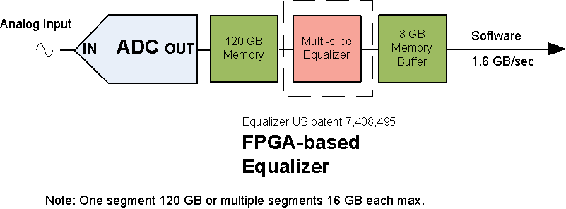
Figure 3: Accelerated Baseband Filtering as part of ADC6000 digitizer FPGA.
Note: ADC_BB option license is required to enable the Accelerated Baseband Filtering
Digitizers with Real-Time Baseband Filtering
To increase acquisition time for longer signals, which have smaller analog bandwidth than the digitizer, the Real-time 10 GSa/s baseband digital filtering and decimation option can be used to reduce acquisition data and increase ENOB before storing it to the memory. This option enables triggered streaming and recording of up to aggregated 1.25 GSa/s or 500MHz of baseband with the ADC6044 across all channels together with the segmented memory option. In 10 Gsa/s mode the ADC6000 digitizer the Real-Time Baseband filtering is implemented using FPGAs (Figure 4).

Figure 4: Real-Time Baseband Filtering as part of ADC6044 digitizer FPGA.
Note: ADC_BBRT1 option license is required to enable the Real-Time Baseband Filtering
Digitizers with patented multi-slice equalizer
The equalizer is used to reduce misalignment between interleaved ADC-s inside of high speed digitizer. (Figure 5) shows the main effect of the equalizer, which is to increase the SFDR of the 40 Gsa/s digitizer with instantaneous 13 GHz of analog bandwidth. The equalizer also corrects amplitude and phase frequency responses of digitizer. Refer to Equalization of Multiple Interleaved Analog-to-Digital Converters (ADCs) white paper for more detail.
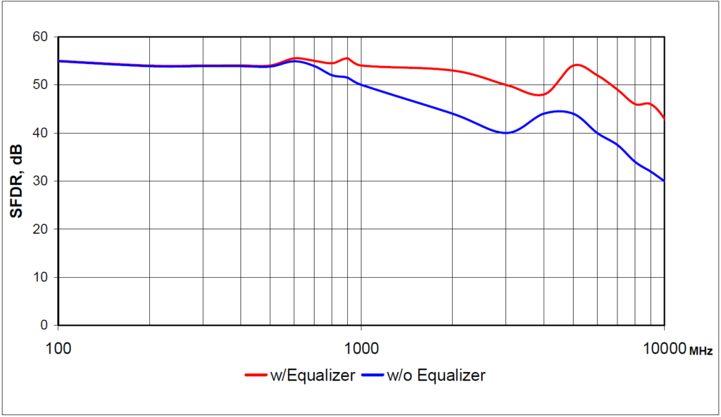
Figure 5: 13 GHz, 40 Gsa/s, 8-Bit Digitizer normalized SFDR vs. Frequency
(Figure 6) shows the equalized frequency response and (Figure 7) shows the step response of ADC6131 digitizer. The careful equalization reduces requirements for post equalization in I/Q channels.
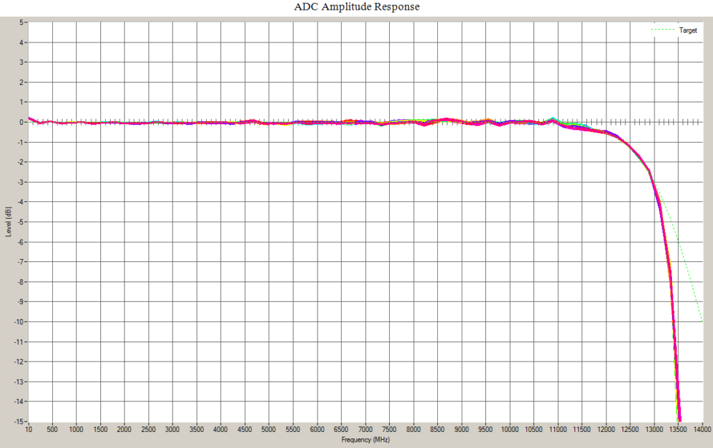
Figure 6: 13GHz, 40 Gsa/s, 8-Bit Digitizer Equalized Frequency Response
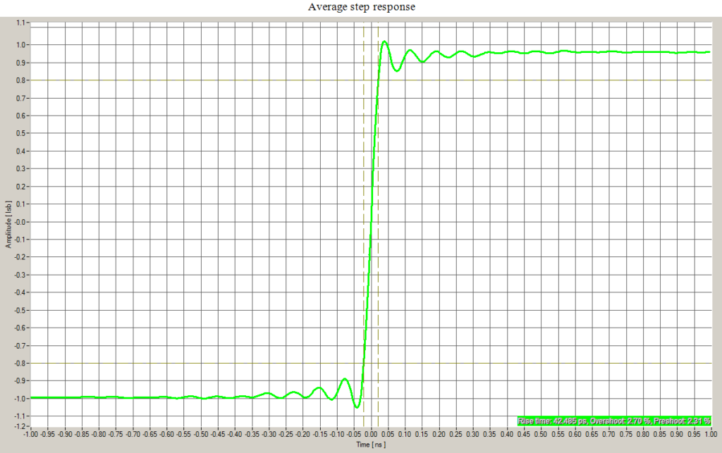
Figure 7: 13GHz, 40 Gsa/s, 8-Bit Digitizer Equalized Step Response
The maximum FPGA-accelerated DDC analysis span is 7.8125 GHz for (ADC6131 40 Gsa/s ), 3.90625 GHz for (ADC6082 and ADC6044 20 Gsa/s ) and 1.953125 GHz for (ADC6044 10 Gsa/s ). The frequency resolution of the local oscillator (LO) of the FPGA-accelerated DDC is 0.0023 Hz (ADC6131 40 Gsa/s ), 0.0011 Hz (ADC6082 and ADC6044 20 Gsa/s ) and 0.0006 Hz (ADC6044 10Gsa/s ).
As mentioned above the bandwidth at down converter output is significantly smaller compared with the bandwidth of digitizer itself. As a result, noise level is reduced and ENOB is increased. If span of analyzed signal is, for example 4 times smaller compared with digitizer bandwidth, the ENOB is increased by 1 bit.
(Figure 8) shows how ENOB changes versus span of digital down conversion at center frequency 3.9 GHz.
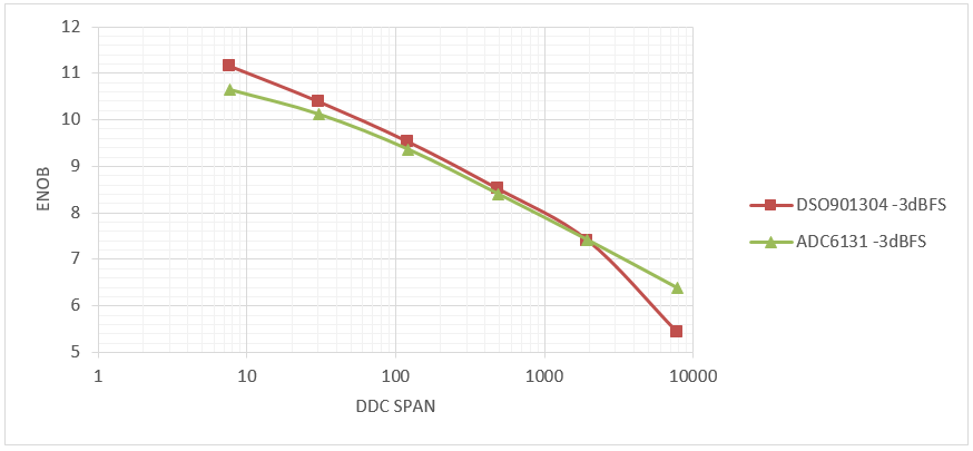
Figure 8: Effective Number of Bits (ENOB) versus DDC Span for one ADC6131 digitizer compared to one DSO 901304 using Keysight VSA 89600 software. Note: Measurement results provided are representative and may vary from instrument to instrument.
(Table 9) lists results of EVM measurements for different modulation standards using the Keysight N5182B VSG or M8190A AWG as a signal source.
| Digitizer | Standard | Center Frequency GHz |
DDC Analysis Bandwidth MHz | Typical EVM dB (%) |
| ADC6131 | QPSK | 2.5 | 4800 | -38 dB (1.24%) with pre-corrections |
| Multi-tone QPSK | 1 and 3 | 1600 | -39.2 dB (1.1%) with pre-corrections |
|
| 802.11ad (MCS1) | 5 | 2500 | -36 dB (1.6%) without corrections |
|
|
802.11ad (MCS1) |
2.5 | 2500 | -39.2 dB (1.1%) without corrections |
|
| 802.11ac | 5.8 | 160 | -42 dB (0.8%) without corrections |
|
| 80 | -43 dB (0.7%) without corrections |
|||
| 40 | -44.4 dB (0.6%) without corrections |
|||
| 20 | -46 dB (0.5%) without corrections |
|||
| LTE-A FDD | 1 | 20 (QPSK) | -50.5 dB (0.3%) without corrections |
|
| 20 (16QAM) | -50.5 dB (0.3%) without corrections |
|||
| 20 (64QAM) | -50.5 dB (0.3%) without corrections |
Table 9: EVM% versus modulation standard. Signal source Keysight MXG N5182B VSG used for 802.11ac and LTE. M8190A AWG used for QPSK and N5152A mode used for 802.11ad. Note: Measurement results provided are representative and performed under ideal conditions.
FPGA-accelerated Baseband and I/Q measurements
In the 5 slot AXIe M9505A 4U chassis up-to two I+jQ 13 GHz (ADC6131), five I+jQ 8 GHz (ADC6082) or ten I+jQ 4 GHz (ADC6044) channels can be formed. If bandwidth of I/Q signals is smaller than the digitizer bandwidth, the BB digital filtering and decimation is used to increase ENOB and reduce data amount needed to be transferred to the PC for processing. Please note, maximum eight I+jQ channel analyzer can be formed in the Keysight 89600 VSA software.
Multi segment acquisitions in the Digitizers use a circular acquisition buffer with minimum inter-segment dead-time of 300nS. This allows for example to capture repetitive signals with relatively large repetition intervals and better utilize the already large acquisition memory, by discarding dead-time in between signals. (Figure 10)
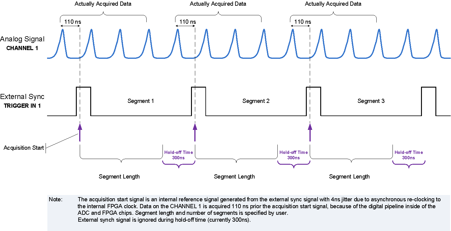
Figure 10: Multi segment acquisitions with pre-trigger
Note: ADC_BB option license is required to enable FPGA-accelerated Baseband functionality. ADC_SM option license is required to enable fixed length Segmented Memory functionality.
ADC6000 Real-Time averaging
Averaging for noise reduction is used in measurements when high dynamic range is required. Averaging is done in real-time in FPGA-s thousands of times faster compared to other methods. With the 40 bit internal accumulator the accuracy of measurements is greatly increased, you can view side bands spectral re-growth and other repetitive signals previously hidden in the noise. The signal to be tested must be repetitive and the repetition rate must be known (The digitizers support up-to 40MHz repetition rate). The time bases of the test signal source and the digitizer must be synchronized and the period must be divisible by 4nS (Figure 11). This will enable the averaging to be stable enough for up-to 4 billion of averages to be performed.
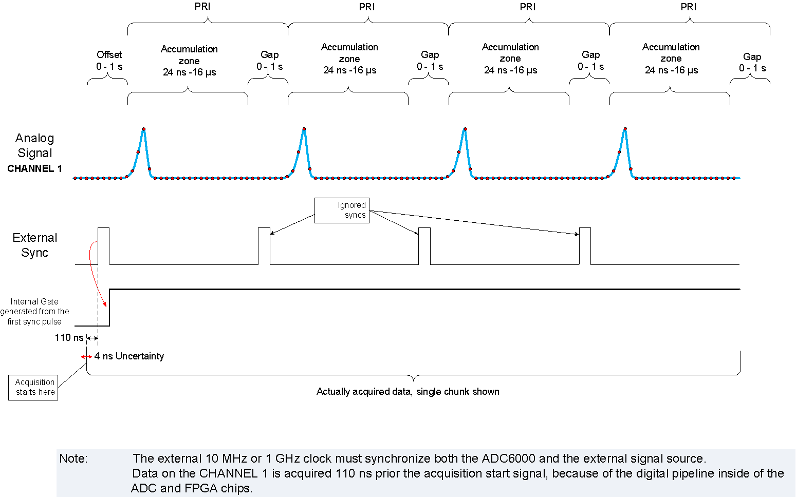
Figure 11: Single-Segment “One-shot” FPGA-based real-time averaging
Note: ADC_AVG option license is required to enable this functionality.
ADC6000 Real-Time segmented averaging
Segmented averaging mode further advances the measurement flexibility by utilizing groups of data of interest into so called “Segments”. Each segment may either have its own trigger event programmed or just suspend the data accumulation process for specified period of time (Segment Gap). Moreover, in Multi-Segment Averaging mode intermediate values of accumulated data may be stored into the digitizer circular memory buffer after each programmed Segment. Data accumulation may be programmed to restart on start of each next Segment or to continue successive data accumulation with the previously accumulated results. See (Figure 12 and 13) for Multi-Segment Averaging timing diagrams.
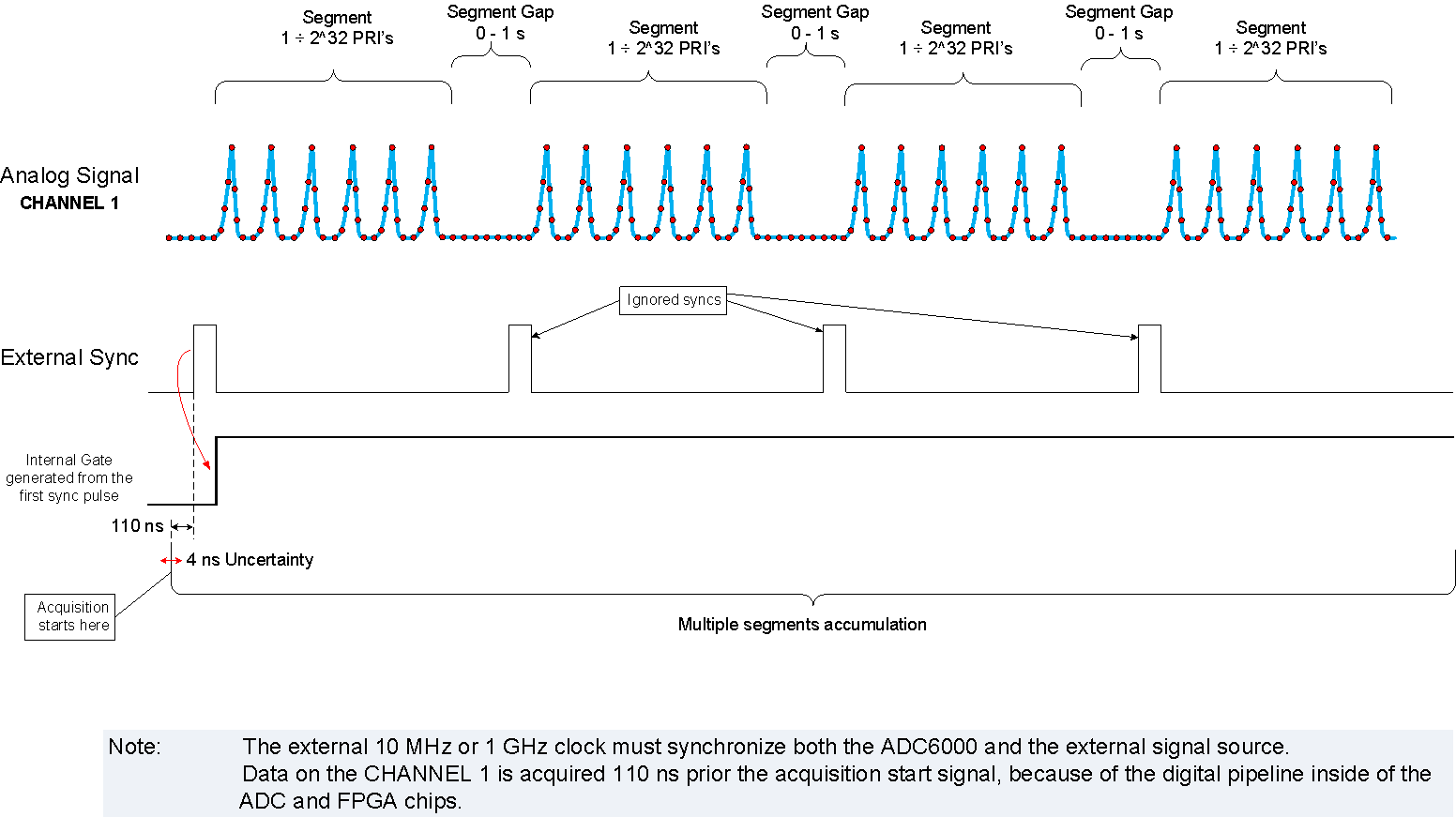
Figure 12: Multi-Segment FPGA-based real-time averaging
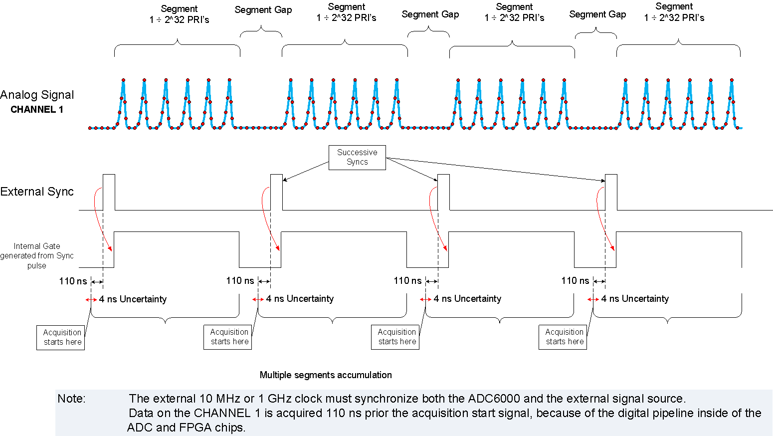
Figure 13: Multi-Segment FPGA-based real-time averaging with external trigger/sync.
Note: ADC_AVGS option license is required to enable this functionality.
ADC6000 Multichannel coherent acquisitions
Digitizers have a possibility for external sampling clock synchronization.
Frequency Synchronization
The frequency synchronization is used to make sure the modules run at the same sample rate, which must be derived from the same master oscillator for all modules. There are two ways to achieve frequency synchronization:
- Feed all modules externally with a common reference clock. The common reference clock can either come from an external clock generator or one module can act as a master and the clock is star distributed to itself and the other ones using the REF IN and REF OUT connectors.
- Feed all modules externally in a star configuration with a common 10 MHz to 10 MHz In, 50 MHz to Ref In, or 1 GHz clock to the Spare front panel connector, which can be configured internally to accept the 1 GHz clock source.
Time Synchronization
All modules must be started at the same time and run with a repeatable skew. Repeatable skew means it stays the same across multiple acquisitions and is maintained across changing sample rate and power cycles. You must have purchased the ADC_SYNC1 option to start the modules with a repeatable skew.
- You can feed all modules externally with a common reference clock. The common reference clock can either come from an external clock generator or one module can act as a master and the clock is star distributed to itself and the other ones using the Ref In and Ref Out
- Alternatively, you can feed all modules externally in a star configuration with a common 10 MHz to 10 MHz In or 50 MHz to Ref In. Configuring the 1 GHz clock to the Spare front panel connector is not supported in this mode.
- For the other digitizers to trigger after the Master, the Test 1 connector should be distributed to all Slave digitizers also in a star configuration. This setup ensures that the Slave digitizers start with a repeatable skew.
- The procedure is to acquire test waveforms that are used to measure the skew between the inputs of multiple modules during a test run.
- Once the skew values are known, the waveform delays can be adjusted to compensate for the measured skew using timestamps. This configuration can be used for MIMO and antennas array measurements.
Note: ADC_SYNC1 option license is required to enable this functionality.
Application samples:
RF engineers familiar with the Keysight 89600 VSA software user-interface, can easily setup traditional measurements with the digitizer or use their existing setup files. The digitizer performs the measurements, FPGA pre-processes them and the results are then displayed in the VSA software. RF/microwave spectrum, frequency, phase characteristics, EVM measurements and many Satcom and other modulation standards like QPSK, 16QAM and 64QAM are available. An example of wideband QPSK can be seen below: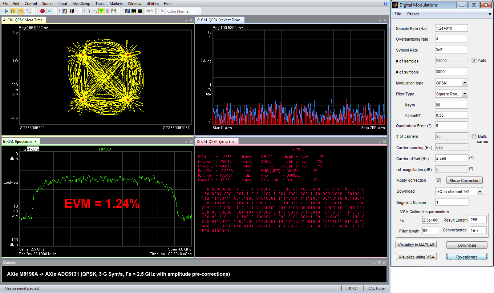
Keysight 89600 VSA Software allows for shared channel multi-measurements, which otherwise would require an additional vector signal analyzer or an extra RF channel. Below is a multi-tone wide QPSK with an additional full span spectrum analysis trace running simultaneously: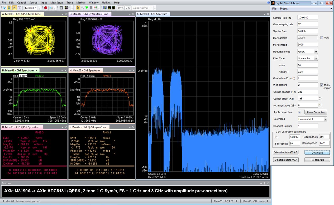
Below is an Keysight M8190A IQ Tools generated 16uS, 0-5 GHz linear chirp, acquired from the AXIe ADC6131 digitizer: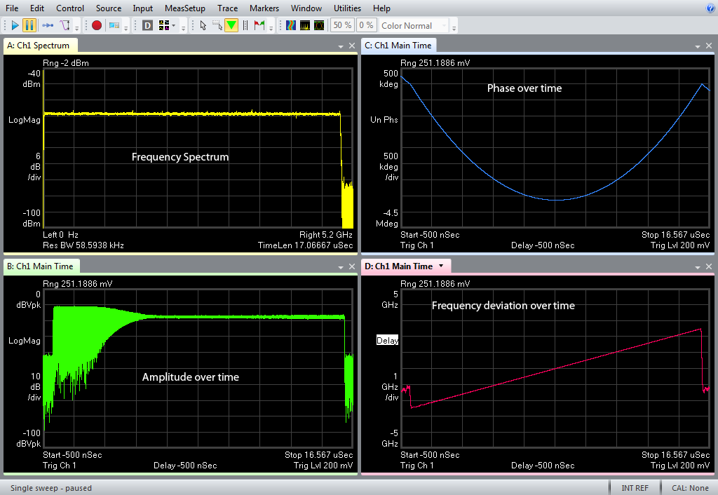
Below is an Keysight M8190A/Speed Mode generated 802.11ad (MCS 1) modulation centered at 2.5 GHz, acquired from the AXIe ADC6131 digitizer: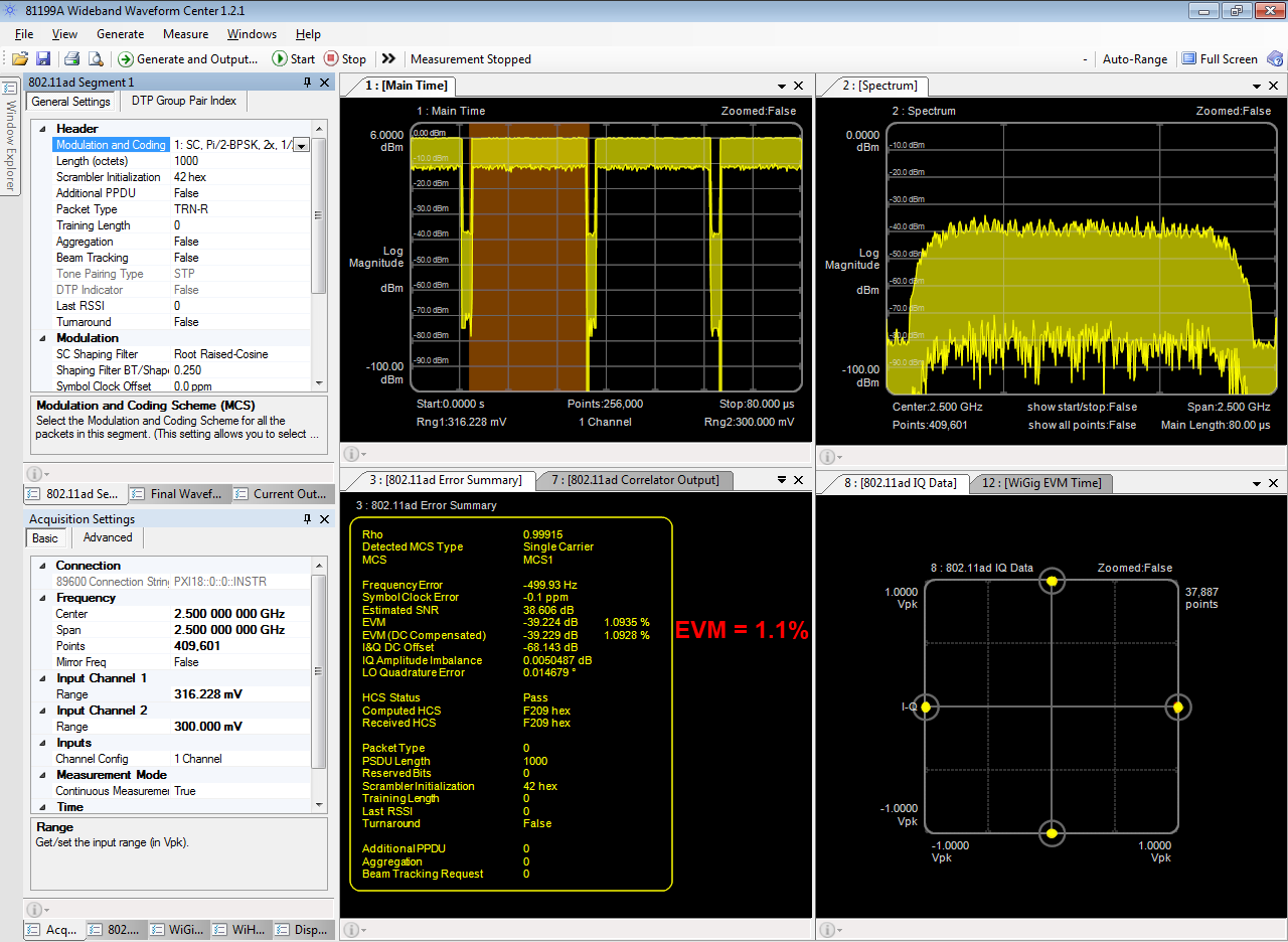
Below is an Keysight M8190A/N5152A mode generated 802.11ad (MCS 1) modulation centered at 5 GHz, acquired from the AXIe ADC6131 digitizer: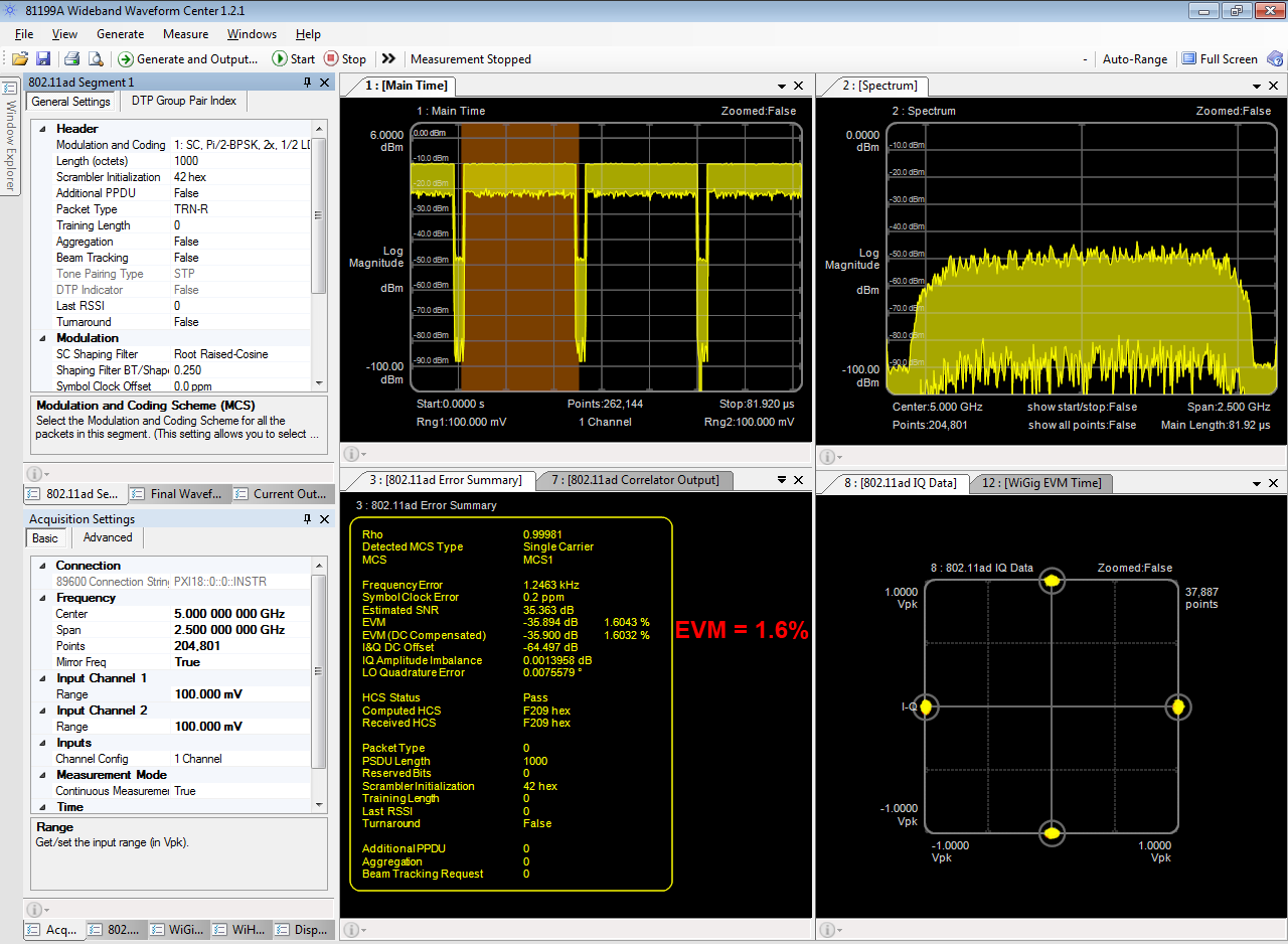
Note: Application Sample measurement results provided are representative and performed under ideal conditions. The results are not warranted specifications.
Please be sure to check out www.keysight.com to find out more about the software compatible with Guzik ADC6000 Series digitizers.

