ADP7104
10 GHz, 10-Bit Streaming Digitizer
Key Features
- 2 channels at 32 GSample/s
- 4 channels at 16 GSample/s
- DC to 10 GHz analog bandwidth
- Measure signals with 28 ps rise times
- 10-bit resolution
- 256 GByte of memory (3.2 s per channel)
- 16 mV to 8 V input (55 calibrated ranges)
- 80 GSa/s sustained streaming
- Signal averaging with 99% trigger efficiency
- Digital down converter with zero overhead
- Dedicated high precision external trigger
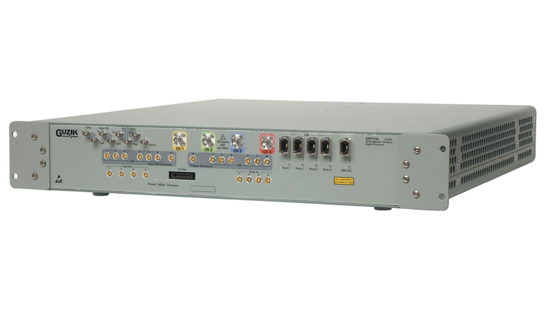
Guzik ADP7104 High-Performance Digitizer and Digital Processor combine high-speed waveform digitizer with built-in digital signal processing, which both enable mixed-domain signal capture and analysis with high-speed data transfer links to computers. The ADP7104 comes in a display-less 2U high 19” rack mountable Guzik enclosure form factor.
The product addresses demanding Electronic Test and Measurement (ETM), Automatic Test Equipment (ATE) and Original Equipment Manufacturer (OEM) systems applications in advanced research such as 5G, wireline and wireless communications analysis, hydrodynamics, plasma fusion, scanning electron microscopy (SEM), mass spectrometry (MS), fourier transform ion cyclotron resonance mass spectrometry (FT-ICR MS), time of flight mass spectrometry (TOF–MS), matrix assisted laser desorption/ionization time of flight mass spectrometry (MALDI-TOF), inductively coupled plasma mass spectrometry (ICP-MS), thermal ionization mass spectrometry (TIMS), liquid chromatography (LC-MS), gas chromatography (GC-MS), ion mobility mass spectrometry (IM-MS), electron spin resonance (ESR) rotational spectroscopy, semiconductor, asynchronous and synchronous contactless Electro-Optical voltage Probing (EOP), Visible Laser Probing (VLP), Laser Voltage Probing (LVP), Laser Time Probing (LTP), Laser Scanning Microscopy (LSM), Laser Voltage Imaging (LVI), Photon Emission (PEM), physics, astronomy, aerospace, defense, avionics, military, radar electronics and a variety of other disciplines. The wide analog bandwidth and high sampling rate of the digitizers provide multi band coverage on multiple input channels. For example, the direct RF-sampling capabilities of the digitizers cover radar signals in HF, VHF, UHF, L-, S-, C-, and part of X-band. Direct RF-sampling reduces the overall system complexity by eliminating several input analog down-conversion stages.
The ADP7104 digitizer feature 10-bit Keysight Analog to Digital A/D converters with sampling rates up to 2 x 32 Gsa/s and analog bandwidth DC to 10 GHz with range adjustable front end (-32 dBm to +22 dBm with 1 dB steps). The ADP7104 with up to 256 GBytes of acquisition memory, delivers the longest waveform capture time window available in a high bandwidth analog to digital converter instrument.
ADP7104 features an FPGA-based reconfigurable digital signal processor with up to 2 channel 32 Gsa/s combined processing speed to convey massive time-critical computations directly inside the instrument.
The PCI Express Gen 3 link provides fast control access and DMA transfer of the acquired data to the host computer’s GPU and CPU-based processing back-end. The PCIe Gen 3 x8 link delivers up to 5 GByte/s of user data transfer rate. In addition, four dedicated Optical Data Interfaces can be configured for Real-Time Continuous Streaming to DP9000, host PCs or RAIDs at up to 2 x 32 Gsa/s (80 GByte/s).
A Software Development Kit is supplied to control the instrument and to integrate the ADP7107 into an existing measurement system. Guzik also supplies Signal Display Soft Front Panel graphical interface application for signal capturing and visualization.
The block diagram below shows the main components of the modular instrument:
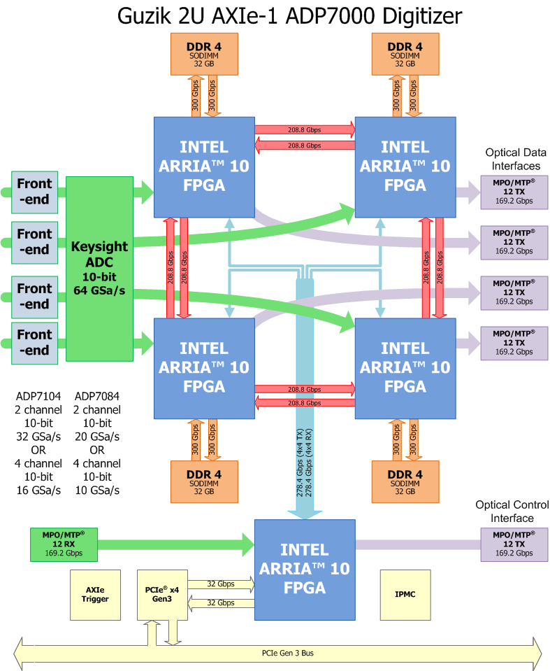
Figure 1. Block Diagram of ADP7000 Module
Guzik ADP7107 Digitizer
ADP7104 |
|
| Input Channels | 4 |
| Analog Bandwidth (-3dB) |
10 GHz (2-ch mode) 6.5 GHz (4-ch mode) |
| Sampling Rate (per channel) |
32 Gsa/s (2-ch mode) 16 Gsa/s (4-ch mode) |
| Acquisition Memory1 (per channel maximum) |
104 Gpts (2-ch mode) 52 Gpts (4-ch mode) |
| PCI Express Gen 3 Interface to AXIe chassis | X4 standard |
________________
1 With 15/16 memory utilization and 256 GByte memory
Data Acquisition System
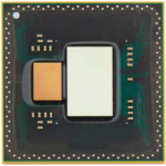
At the heart of the ADP7107 digitizer is state of the art high-speed real-time 10-bit analog to digital converter (ADC) ASICs supplied by Keysight Technologies, which provide high speed waveform capture with 4x more vertical resolution and better SNR than 8-bit ADC-s.
A low-noise front-end amplifier/attenuator is connected to each input channel, which enables user selectable wide operational vertical input range.
The patented2 Guzik digital frequency response equalization further improves the signal fidelity and effective number of bits.
At the maximum sampling rate of 32 Gsa/s (31.25 psec per point), the ADP7104 can capture up to 3.2 seconds of a real-time waveform into its ultra-long acquisition memory per channel in two channel mode.
________________
2 U.S. Patent 7,408,495
Internal Clock
Internal clock accuracy is critical for deep-memory applications. The multi channel digitizers achieve precise time accuracy with a next-generation premium ultra low phase noise time base architecture. Time scale accuracy of (50 parts per billion versus Temperature) after calibration and down to 50 fs of intrinsic jitter.
Channel Trigger
The ADP7104 digitizer features a digital processing trigger. This feature makes use of the real-time hardware waveform processing capability and allows you to define trigger parameters based on the actual digital waveform data. This trigger is available on any input channel. In addition, four external trigger/gate source inputs are provided. Trigger conditions are set using the Signal Display software tool or from your application via SDK.
Processing Overview and Capabilities
ADP7104 digitizer provide various options for signal processing: FPGA, GPU, and CPU-based processing.
FPGA-Based Processing

Inside the ADP7104 digitizer are four Intel Altera ArriaTM 10 FPGAs for processing. These core processing elements combined with Guzik’s implementation of customer-specified measurement algorithms provide end users with a truly tailored measurement solution where speed and throughput count.
The FPGA-based processor combined with Guzik’s custom engineering capabilities provides you with the possibility to perform digital signal processing directly in ADP7104 digitizer prior to sending waveform data out to computer. Many applications may require only processed results to be sent to the host computer rather than raw waveform data. Guzik can work directly with customers to implement custom processing capabilities drawing from years of experience in waveform analysis. Choice of firmware options includes channel equalization, filtering, multi-segment time-tagged acquisition, Real-Time Digital Down Conversion (DDC), Fast Fourier Transform (FFT), Discrete Fourier Transform (DFT), waveform min/max, Real-Time Waveform Averaging, and parameter calculations among others are all available along with application-specific requests. Guzik can provide custom services after a technical consultation regarding the specific application and required processing.
The combined FPGA processing resources are listed in the table below:
Processing Block |
Number |
Notes |
| Logic Cells | 2,640,000 | Logic Elements |
| Block RAM |
8,532 168 |
M20K memory blocks M20K memory (Mb) |
| Multipliers | 13,504 | 18-bit x 19-bit multipliers |
Real-Time Digital Down-Conversion (DDC) with de-embedding equalizer and IF Magnitude trigger
The Guzik ADP7104 10-bit 16/32 Gsa/s digitizer can directly sample RF signals at DC to 6.5 GHz on four channels or DC to 10 GHz on two channels simultaneously and in Real-Time Digitally Down-Convert (DDC) the signals to digital I-Q baseband.
The digital down-conversion FPGA block diagram, equalization filtering, re-sampling and decimation process is shown below:

The patented digital down converter with an equalizer translates an ADC output signal to a low frequency spectral region, followed by decimation. All operations of correction of the processed signal are carried out with a reduced sampling rate compared with sampling rates of the prior art. Equalization is performed only in a frequency pass band of the down converter. The achieved reduction of the required computation resources is sufficient to enable the down converter with equalization to operate in a real time mode at up to 32 Giga samples per second (Gsa/s).
The data from the ADC is transferred directly to the DDC with digital equalizer, then to the memory and from memory to the analysis software. The down conversion is implemented by two multipliers with Sin/Cos LO signals. The LO signals area created per channel settable with a 44-bit Numerically Controlled Oscillator (NCO) design inside the FPGA-s and allows to set the DDC center frequency per channel with 0.0018 Hz resolution for 32 Gsa/s and 0.0009 Hz for 16 GSa/s mode.
Down converted signals connected through LPF/decimator to I/Q memory and are then transferred to PC.
Real-Time DDC per channel settable user-span has a 1 Hz setting resolution and has an oversampling factor of 1.28x. For a signal with 1 GHz user-span the DDC output data-rate is 1.28 GSa/s. Each sample pair of I & Q is coded on 16/32 bits (8/16-bit I and 8/16-bit Q). For every user span bandwidth reduction by four, the signal to-noise ratio (SNR) is improved by 6 dB or 1 bit of vertical resolution.
The Real-Time IF magnitude trigger allows setting a level the signal needs to achieve at a specified center frequency per channel and allows the data for the signal of interest to pass to the I/Q memory this allows to Start and Stop Variable Length Segments on the IF Magnitude.
In many applications input signal can be easily down converted with the use of up-front analog down converter to the Intermediate Frequency (IF) within the analog signal bandwidth of the ADP7104. The digital de-embedding equalization technology can then be extended to external mmWave down-converters which are working together with the wideband digitizer to create a calibrated receiver.
Note: ADC_ADDCRT1 option license is required to enable the Real-Time DDC, ADC_BB option license is required to control the de-embedding equalizer and ADC_VSM1 option license is required to enable Variable Length Segment Mode. Maximum supported Real-Time down converter user span for the modulated signal is 2.5 GHz in 16G/32 Gsa/s mode (ADP7104) and 1.56 GHz in 10/20 Gsa/s mode (ADP7084).
Real-Time Stream Processing Architecture via Fiber Optics
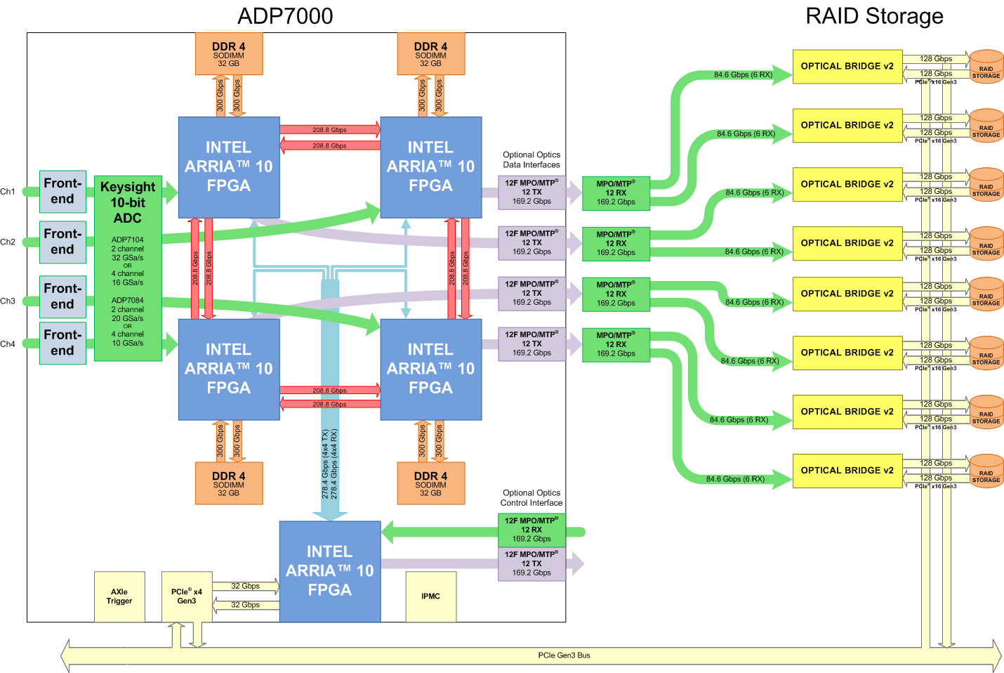
The ADP7104 digitizer introduces Real-Time Stream Processing Architecture via fiber optics interconnect technology. It allows to cascade additional DP9000 processors together with the ADP7104 digitizer to achieve higher memory capacity and processing capabilities.
Combined with the Optical Bridge Interface Card the DP7000 can be connected to external PC-s and RAID arrays via the fiber optics interconnect technology.
Continuous streaming to additional DP7000-s, host PCs or RAIDs at up to 640 Gbps is shown in the block diagram illustrating the connections and data throughput:
PCI Express Host Computer Control Interface

The ADP7104 provides PCI Express Gen 3 x4 and x8 interface. The PCI Express bridge card installs into the host computer, and a standard PCI Express x8 cable connects the AXIe chassis to the host computer.
High speed waveform transfer with sustained user data rates up to 5 GByte/sec is possible from this port back to the host computer.
GPU-based Processing
 General-purpose computation on graphic hardware allows developers to reuse the computational algorithms available for GPU or develop their own algorithms on CUDA C or OpenCL. NVidia® GeForce GTX 10804 GPU can be shipped as an option with the ADP7000. It is possible to use any NVidia® GPU with computing capability 2.0 or higher, if its power requirements are satisfied by the computer.
________________
4 Current configuration. More powerful GPU cards may be shipped in the future
CPU-based Processing
 In addition to FPGA-based and GPU-based computation, customers have an option to perform signal processing using a computer CPU. Multi-core processing libraries, such as OpenMP, allow utilizing full power of modern 12-core CPU computers. Once more powerful computers with additional cores are released, you can upgrade your computer keeping your existing ADP7000 Digitizer Module.
Ultra-fast GPU-based FFT Measurements5
ADP7104 digitizer performs frequency domain analysis using the Fast Fourier Transform (FFT) calculated on a GPU. Single NVIDIA® GTX GPU card performs FFT calculations at a 2.5 Gsa/s processing speed. This means, for example, that collecting data at 10 Gsa/s for 100 µs, processing in 400 µs, the full signal spectrum up to 5 GHz with resolution bandwidth 10 kHz – 500,000 spectral lines would take less than 0.5 ms.
________________
5 Available using the Software Development Kit (GSA SDK)
Temperature Stabilization
The ADP7104 digitizer modules keep constant temperature for the critical A-to-D components for better measurement accuracy. Tested at ambient temperatures from 15°C to 35°C in standard AXIe chassis.
External Clock and I/O

The ADP7000 Modules feature 50 ohm SMA connectors for inputs and MCX connectors for clock, external gate and control I/O connections.
One Synchronization Clock Input and Output. The Synchronization Clock Input supports 50 MHz, 100 MHz or 200 MHz reference clock frequencies. The front-panel built-in Synchronization Clock Distributor allows precise time synchronization of more than one digitizer to increase the number of phase coherent digitizer channels available in a system.
One ADC 1 GHz Reference Clock Input and Output.
Four Gate Inputs are available to trigger the instrument from external control signals or markers.
Four Test Outputs are available for custom application support and system integration.
External I/O dynamic scenario port provides real-time control access to processing
FPGA’s. Precise DDC carrier frequency, phase and amplitude settings are possible in real-time through the sequencer control. Complex operations such as frequency sweeps are possible.
ADP7000 provides a programmable built-in calibrator with a variety of test signals. Automatic calibration routine is run during every application start while initializing the sub-systems to ensure accurate operation of the instrument. In addition, the calibrator signals can be user switched to output the test signals to the front panel output connector.
Please contact us for more information.
GSA Toolkit Software, Keysight Frequency and Time Domain Measurement and Analysis Software
Guzik provides a GSA Toolkit to control the ADP7104 digitizer, which includes three software components:
- Interchangeable Virtual Instrument (IVI) Digitizer Compliant Instrument Driver
- GSA SDK – software development kit to create custom standalone applications for ADP7104 or to integrate ADP7104 into an existing software environment; please refer to “Guzik Signal Analyzer Software Development Kit User’s Guide” document P/N 02-107544 for more details.
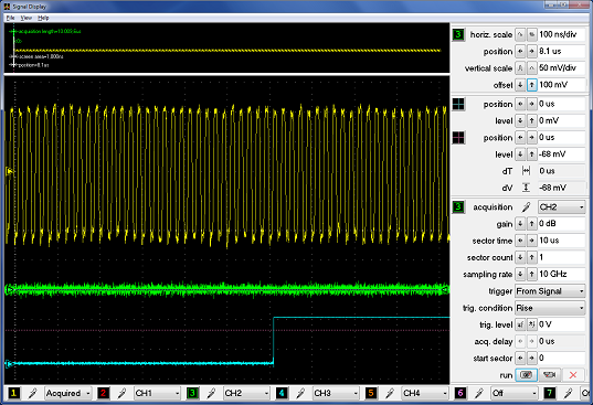
- Signal Display application designed for easy instrument setup, waveform acquisition and visualization. Signal Display provides oscilloscope-like graphical user interface to display multiple signal waveforms, control acquisition parameters (sampling rate, duration, trigger settings, etc), and perform multiple trigger (multi-sector) acquisitions. The application allows for saving acquired signals to the computer storage. You can also load and display signals from files in various formats, including the previously saved waveforms. One of the useful features of Signal Display is tracking (monitoring) acquired signals during GSA SDK-based application execution. Please refer to “Signal Display User’s Guide” document P/N 02-107548 for more details.
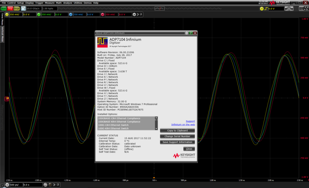
Guzik ADP7104 Digitizers integrate seamlessly with the following Keysight Software Packages to provide live connectivity for hardware accelerated Frequency and Time Domain Measurement and Analysis capabilities.
Infiniium Hosted Oscilloscope Interface Software for Digitizers (N8901A)
Key Features & Specifications
Productivity
- Use your PC to view and analyze to get additional insight, without having to be with your scope and target system.
- Share scope measurements more easily across your team, and if needed with customers and vendors.
- Create more useful documentation, faster.
- Supports a variety of popular file formats from Keysight Infiniium and InfiniiVision oscilloscopes as well as generic .csv, .txt, and .tsv files.
Standard Features
- Open and view up to 8 waveforms (supports up to 16-bit vertical bits)
- Use familiar scope horizontal and vertical controls to quickly navigate and zoom in to any event of interest
- Access over 60 built-in automated measurements with a mouse click.
- 20 math operators including FFT and filters, up to four independent/cascaded math functions
Optional Features
- Protocol decode (I2C, SPI, RS-232, CAN, LIN, FlexRay, JTAG, USB, PCIe, MIPI D-Phy, 8B/10B, SAS, SATA…)
- Jitter analysis with EZJIT and EZJIT+
- Eye analysis and clock recovery for high-speed serial
Licensing
- Requires a License from Keysight
More information at www.keysight.com/find/InfiniiumUserInterface
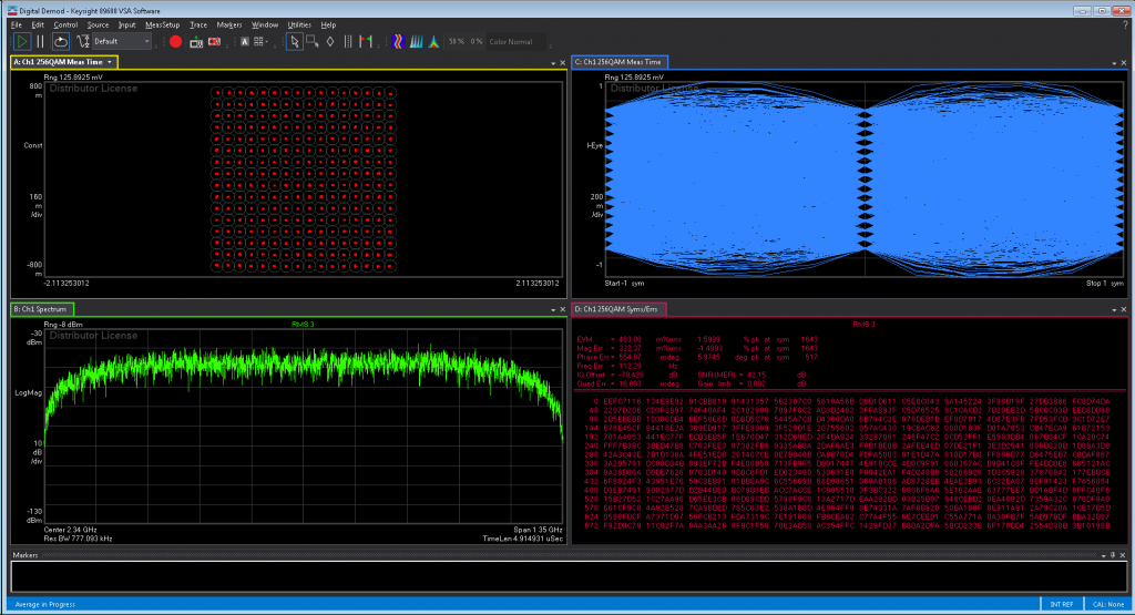
Vector Signal Analyzer Software (89600 VSA and WLA)
Overview
Software tools to explore every facet of a signal and optimize your designs.
Measure a broad range of signals including 5G, IoT, radar and more.
Gain greater insight in frequency, time and modulation domains.
Licensing
- Requires a License from Keysight
More information at http://www.keysight.com/find/89600
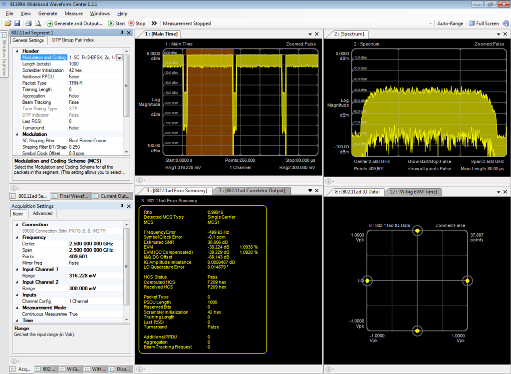
Wideband Waveform Analyzer (81199A)
Key Features & Specifications
- Standard-compliant waveform generation. Libraries are available for Wireless HD, WiGig, IEEE802.11ad and IEEE802.11ay
- Complete high precision testing
– Signal simulation on the transmitter side
– Signal analysis on the receiver side - Waveform creation using simple drag and drop actions
- Measurement results at a glance. All important results can be configured on one screen. A color-coded composite constellation display allows fast detection of problems.
- Simple drill down to possible parameters.
- Calibration routines for optimizing performance of devices.
- For usage with Arbitrary Waveform Generators M8190A, 81180B and M8195A.
Description
The trend continues: Increasingly convenient wireless access is driving demand for more data in less time. As transmission rates climb, it puts additional strain on components, infrastructure, frequency spectrum and developers. The demand for wideband data is also inspiring the creation of new standards that utilize increasingly complex modulation schemes to transmit more data through the available spectrum.
To help you keep pace with higher frequencies, wider bandwidths and new standards, Keysight has created the 81199A Wireless Waveform Center software. Key elements include the Wideband Waveform Creator signal-generation application and the Wideband Waveform analyzer application. Both support emerging wideband modulation formats such as
- Wireless HD,
- WiGig and
- IEEE 802.11ad
- IEEE 802.11ay
81199A simplifies the test challenges for 60 GHz wireless tests
- Compliant testing for Wireless HD, WiGig, IEEE802.11ad & IEEE802.11ay
- Complete transmitter and receiver testing
- Simple signal generation simple with drag & drop creation
- Modulation analysis at a glance of fully coded signals
- Addresses the challenge of 2 GHz and 4 GHz modulation bandwidth
– 100 times wider bandwidth than 802.11n
– 1.5 times wider bandwidth than 802.11ac
Licensing
- Requires a License from Keysight
More information at www.keysight.com/find/81199A
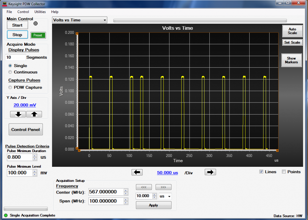
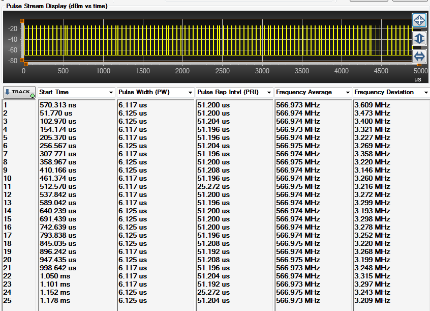
Keysight PDW Collector Software (PS-X10-100)
Key Features & Specifications
- Convert RF Pulses to Pulse Descriptor Words (PDWs)
- 1, 2, or 4 RF Channels
- Dynamic range of > 60 dB
- Operating range of +22 dBm to -32 dBm
- Frequency range set by ADP7000 digitizer
- Rapidly Collect and Process Data
- Designed to work in a dense RF environment
- Fast capture and Off-Load time
- Variable Segmented Acquisition Capture Support
- Deep Acquisition Memory, 128 GB per module (256 GB future)
- Real-Time up-to 2.5 GHz/Channel user band DDC Implemented in digitizer hardware for Speed (ADP7104)
- Real-Time DDC with de-embedding equalizer for external converters
- Variable Segment Length with Real Time DDC. Removes any pulse width constraint and adjusts segment length based on incoming pulse signal data.
- Provide Detailed Display, Processing, and Export Tools
- Capture and Display Power, Frequency, and Phase vs Time
- Capture and Process PDW information on large collection of pulses
- Graphical Display of Parameters vs Time or as a Histogram
- Filter, Search, and Determine Statistics on Collected Parameters
- Export PDW results in a *.csv format
- SQL Data-basing of PDW Information
- Remote Interface
- Socket or Scripting Method for Remote Control
- API Description Document Available
Operating Modes
- Pulse Capture and Display
- Power/Frequency/ or Phase vs Time
- Output to GUI graphs
- Single or Repetitive Capture
- Designed for quick checkout and setup
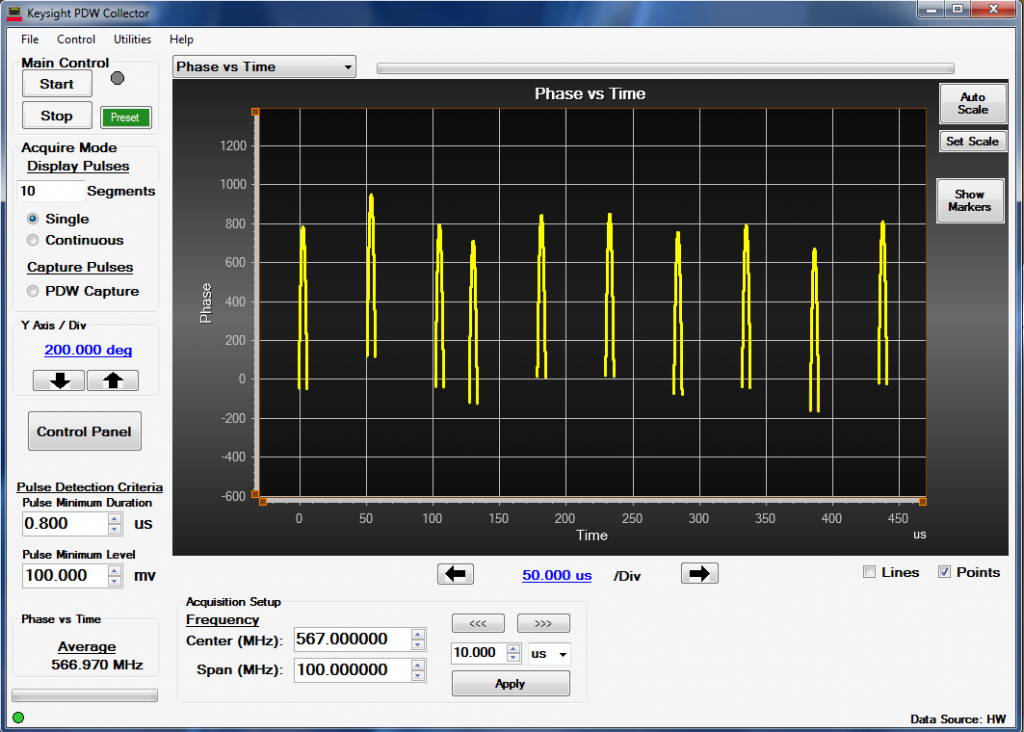
- PDW Capture Mode
- Batch Processing (Acquire/Process/Display)
- Construct PDW information from signal data acquired
- Features
- Plot Parameters and/or Pulses
- Search and Filtering
- Advanced Plotting / Scatter Plots
- Export Results
Licensing
- Requires a License from Keysight
For more information contact sales@guzik.com
Information about the available firmware and software options for the ADP7104:
| Firmware Option | Description |
|
ADC_BASE (Digitizer Base License) |
Base license for one segment simultaneous acquisition and readout of data to the host computer, with patented6 digital Time-Interleaved ADC mismatch, frequency response and phase equalization. Please refer to white paper Equalization of Multiple Interleaved Analog-to-Digital Converters (ADCs) |
|
ADC_SM (Segmented Memory Acquisition) |
Multi segment acquisitions in the Guzik digitizers use a circular acquisition buffer with minimum inter-segment dead-time of 300ns. This allows, for example, to capture up to 64 million repetitive signals with relatively large repetition intervals and better utilize the already large acquisition memory by discarding dead-time in between the repetitive signals. Down to attosecond resolution time-tagging allows to know the precise time between each captured waveform segment. Please refer to GSA SDK User’s Guide section 5.1.2 Acquisition Format Specification |
|
ADC_BB (Baseband Filtering) |
Real-time baseband digital filtering with adjustable bandwidth from 10 GHz and down to 119.18 MHz. When the filter cut-off frequency is reduced by twice or more, the corresponding decimation is applied. The entire frequency range uses decimations from 1 to 64 in powers of 2. Filtering improves SNR and ENOB for signals with bandwidth below 10 GHz. Additionally, filtering below 10 GHz will result in data reduction, which requires less throughput to transfer the data to the host computer. |
|
ADC_ADDCRT1 (Real-Time Digital Down-Converting) |
The Real-Time patented7 16/32 Gsa/s (ADP7104), 10/20 Gsa/s (ADP7084) Digital Down-Conversion option allows to perform the down conversion in real-time in the ADP7000 digitizer FPGAs. Real-time per channel IF frequency and IF Magnitude triggering can be used to decide if data is to be stored to the digitizer I/Q memory or not. This allows to capture and store only signals of interest within the per channel settable DDC span and reduces the data amount needed to be transferred to the PC for post processing. Keysight 89600 VSA software or similar can be used to tune DDC parameters and perform final processing and measurements related to particular transmission standard. Please refer to GSA SDK User’s Guide section 5.8 Performing Digital Down Conversion. The specification is provided lower on this page. |
|
ADC_VSM1 (Variable-Length Segments with ADC_ADDCRT1) |
Variable length segmented memory acquisition allows for segmented capture where each segment has a length optimized to capture RF pulses using the Real-Time IF Magnitude Trigger and have minimal dead time capture. This greatly extends the utility of the memory. Please refer to GSA SDK User’s Guide section 5.9.2 Magnitude Trigger |
|
ADC_AVGA (Real-time Averaging) |
Averaging of a repetitive signal improves the signal-to-noise ratio and reveals small signals otherwise buried in noise. Averaging is performed in real time with an external trigger synchronous with signal source. To achieve precise averaging, the trigger has a lower jitter of <0.8ps RMS. The trigger uses a dedicated input and allows up to all four digitizer channels to be used for averaging simultaneously. The maximum averaging window is 20 microseconds, and the maximum number of averages is > 50 million (with 256 GB memory option). |
|
ADC_AVG (High Speed Deep Averaging) |
Averaging for noise reduction is used in measurements when high dynamic range is required. Averaging is done in real-time in FPGAs thousands of times faster compared to other methods. With the 40-bit 1024K internal accumulator the accuracy of measurements is greatly increased by allowing up-to 4 billion averaged waveforms. This allows viewing side bands spectral regrowth and other repetitive signals previously hidden in the noise. Please refer to GSA SDK User’s Guide section 5.6 Performing Real Time Accumulation Measurement |
| ADC_AVGS (Bundles ADC_SM and ADC_AVG)(High Speed Deep Segmented Averaging) |
Segmented averaging mode further advances the measurement flexibility by utilizing groups of data of interest into segments. Each segment may either have its own trigger event programmed or just suspend the data accumulation process for specified period of time. Please refer to GSA SDK User’s Guide section 5.6 Performing Real Time Accumulation Measurement |
|
ADC_SYNC1 (Multi-Module Synchronization Capability) |
Multi-module synchronization capability, allows to increase the total number of digitizer channels by combining multiple modules into one instrument. The option enables multichannel phase coherent time-tagged input channels to be triggered from common source or independently. Synchronization is performed during digitizer initialization and channel-to-channel skew is restored and maintained between instrument channels. The digitizers can be setup to follow an external 50 MHz, 100 MHz or 200 MHz time base without uncertainty, which is critical for ATE and OEM systems application. Please refer to GSA SDK User’s Guide section 4.5 Synchronization of Several Digitizers and 5.1.17 Synchronous Acquisition |
________________
6 U.S. Patent 7,408,495
7 U.S. Patent 9,641,191
Mapping of Required Options to Licenses and Supported Software
The following table describes available options that can be purchased, the required and optional license or licenses for running each software utility, and the sample utilities that can be run if that product is purchased.
| Option | Required License to Operate | Optional License | Supported Software |
| ADC_BB | ADC_BASE | ADC_SM, ADC_SYNC1 |
GSA Signal Display with Spectrum Display, GSA Acquisition Utility, GSA Multi-Module Acquisition Utility, Keysight VSA 89600, Keysight Infiniium Hosted Oscilloscope Interface Software for Digitizers (N8901A), Keysight PDW Collector Software (PS-X10-100), GSA SDK |
| ADC_SM | ADC_BASE | ADC_BB, ADC_ADDCRT1, ADC_FFT1, ADC_BB, ADC_SYNC1 |
GSA Signal Display with Spectrum Display, GSA Acquisition Utility, GSA Multi-Module Acquisition Utility, Keysight VSA 89600, Keysight PDW Collector Software (PS-X10-100), GSA SDK |
| ADC_AVGA | ADC_BASE | GSA SDK | |
| ADC_AVG | ADC_BASE | ADC_SM | GSA Real-Time Accumulator Utility, GSA SDK |
| ADC_AVGS | ADC_BASE, ADC_SM, ADC_AVG, |
GSA Real-Time Accumulator Utility, GSA SDK |
|
| ADC_ADDCRT1 | ADC_BASE | ADC_BB, ADC_SM, ADC_VSM1 |
GSA Real-Time DDC Utility, Keysight VSA 89600, Keysight PDW Collector Software (PS-X10-100), GSA SDK |
| ADC_VSM1 | ADC_BASE, ADC_ADDCRT1 |
GSA Real-Time DDC Utility, Keysight PDW Collector Software (PS-X10-100), GSA SDK |
|
| ADC_SYNC1 | ADC_BASE | ADC_SM | GSA Signal Display with Spectrum Display, GSA Multi-Module Time-Synchronous Acquisition Utility, GSA SDK |
| ADC_FFT1 | ADC_BASE | ADC_SM, ADC_BB |
GSA Signal Display with Spectrum Display, GSA Spectrum Utility, GSA SDK |
Real-Time Digital Down-Converting Specification
| ADC_ADDCRT1 | Guzik ADP7104 with two 32 GSa/s channels or four 16 GSa/s channels |
|
Decimation factors and frequency resolution
|
10 … 65,536 , in 32 GSa/s mode 5 … 65,536 , in 16 GSa/s mode Resolution: 37 Hz ÷ 0.001 Hz |
| Data rate per channel |
3.2 Gsa/s IQ max (2.5 GHz) , in 32 GSa/s mode 3.2 Gsa/s IQ max (2.5 GHz), in 16 GSa/s mode Arbitrary sample rate below max: (RF DDC user span x 1.28 IQ) |
|
LO frequency
|
10 GHz less 1/2 Span x 1.28, in 32 GSa/s mode 6.5 GHz less 1/2 Span x 1.28, in 16 GSa/s mode |
|
LO Resolution
|
0.0018 Hz, in 32 GSa/s mode 0.0009 Hz, in 16 GSa/s mode |
|
LO Accuracy
|
44-bit Numerically Controlled Oscillator (NCO) |
|
Vertical resolution
|
8-bit I and 8-bit Q data or 16-bit I and 16-bit Q data |
| SNR improvement relative to direct mode | 3 dB per octave of decimation (nom.) |
| Decimation filter passband ripple | Same as full band |
| Decimation filter out of band rejection | 70 dB or better |
| IF Magnitude Trigger and segmentation | Yes |
| Variable length segmentation support | Yes |
| Segment time-stamp resolution | UTC Attosecond (1×10⁻¹⁸ seconds) |
| Real-Time full-band FPGA-based user tunable de-embedding equalizer |
160 tap FIR, in 32 GSa/s mode 160 tap FIR, in 16 GSa/s mode |
Built-in capture memory with Real-Time Digital Down-Converter (ADC_ADDCRT1)
|
Wireless standard – (user-span) |
ADP7104 with 256 GByte on-board memory and two 32 GSa/s channels or four 16 GSa/s channels |
|
Available IQ memory per channel |
16 GSa/ch in 32 GSa/s mode 16 GSa/ch in 16 GSa/s mode (16-bit I & 16-bit Q sample pairs)
32 GSa/ch in 32 GSa/s mode 32 GSa/ch in 16 GSa/s mode (8-bit I & 8-bit Q sample pairs) |
|
802.11ad – (2.16 GHz) DDC data rate per channel – 2.7648 GSa/s IQ
|
5.787 seconds/ch in 32 GSa/s mode 5.787 seconds/ch in 16 GSa/s mode (16-bit I & 16-bit Q sample pairs)
11.574 seconds/ch in 32 GSa/s mode 11.574 seconds/ch in 16 GSa/s mode (8-bit I & 8-bit Q sample pairs) |
|
5G NR – (800 MHz) DDC data rate per channel – 1.024 GSa/s IQ
|
15.625 seconds/ch in 32 GSa/s mode 15.625 seconds/ch in 16 GSa/s mode (16-bit I & 16-bit Q sample pairs)
31.25 seconds/ch in 32 GSa/s mode 31.25 seconds/ch in 16 GSa/s mode (8-bit I & 8-bit Q sample pairs) |
|
5G NR – (400 MHz) DDC data rate per channel – 0.512 GSa/s IQ
|
31.25 seconds/ch in 32 GSa/s mode 31.25 seconds/ch in 16 GSa/s mode (16-bit I & 16-bit Q sample pairs)
62.5 seconds/ch in 32 GSa/s mode 62.5 seconds/ch in 16 GSa/s mode (8-bit I & 8-bit Q sample pairs) |
|
5G NR – (200 MHz) DDC data rate per channel – 0.256 GSa/s IQ
|
62.5 seconds/ch in 32 GSa/s mode 62.5 seconds/ch in 16 GSa/s mode (16-bit I & 16-bit Q sample pairs)
125 seconds/ch in 32 GSa/s mode 125 seconds/ch in 16 GSa/s mode (8-bit I & 8-bit Q sample pairs) |
|
5G NR – (100 MHz) DDC data rate per channel – 0.128 GSa/s IQ |
125 seconds/ch in 32 GSa/s mode 125 seconds/ch in 16 GSa/s mode (16-bit I & 16-bit Q sample pairs)
250 seconds/ch in 32 GSa/s mode 250 seconds/ch in 16 GSa/s mode (8-bit I & 8-bit Q sample pairs) |
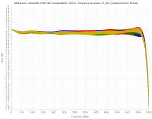
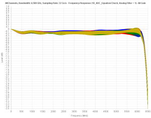
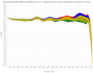
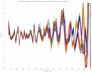
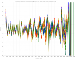
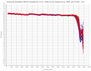
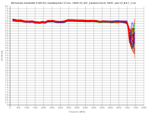
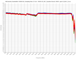
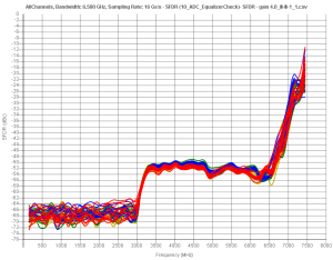
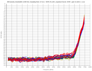
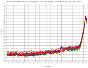
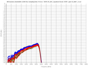
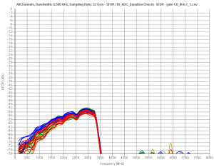
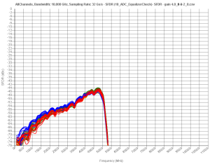
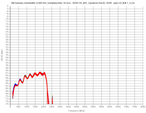
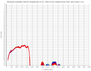
The ADP7104 digitizer have excellent performance characteristics, critical for wideband signal capture.
Production statistics for 40-channels (10 different ADP7104 modules):
- Using digital equalizer: 7,408,495 Digital equalization of multiple interleaved analog-to-digital converters – August 5, 2008
- Group Delay measured using: 9,933,467 Group delay measurement apparatus and method – April 3, 2018
If bandwidth of signal is smaller than the digitizer analog bandwidth, the baseband digital filtering and decimation can be used to increase ENOB and reduce data amount needed to be transferred to the PC for post processing.
| 500 MHz[1] | 1 GHz[1] | 2 GHz | 2.5 GHz | 4 GHz | 6 GHz | 8 GHz | 10 GHz | |
| ENOB, bit, 32Gs/s, | N/A | N/A | 7.7 | 7.5 | 6.9 | 6.7 | 6.5 | 6.2 |
| ENOB, bit, 20Gs/s, | N/A | N/A | 7.4 | 7.2 | 6.8 | 6.6 | 6.4 | N/A |
| ENOB, bit, 16Gs/s, | 8.3 | 7.9 | 7.6 | 7.4 | 6.8 | 6.5 | N/A | N/A |
| ENOB, bit, 10Gs/s, | 8.0 | 7.6 | 7.2 | 7.0 | 6.7 | N/A | N/A | N/A |
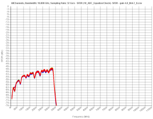
| SFDR, 32Gs/s | N/A | N/A | 70.8 | 68.1 | 69.3 | 67.8 | 65.3 | 65.5 |
| SFDR, 20Gs/s | N/A | N/A | 69.0 | 70.0 | 70.8 | 69.4 | 69.1 | N/A |
| SFDR, 16Gs/s | 70.2 | 67.2 | 67.6 | 66.5 | 67.1 | 64.6 | N/A | N/A |
| SFDR, 10Gs/s | 73.5 | 70.9 | 67.0 | 68.9 | 68.0 | N/A | N/A | N/A |
________________
Note: all limited band measurements with 1 GHz CW, -3 dBFS, -4 dBm / 400 mV full scale
[1] Data measured on 333 MHz input signal.
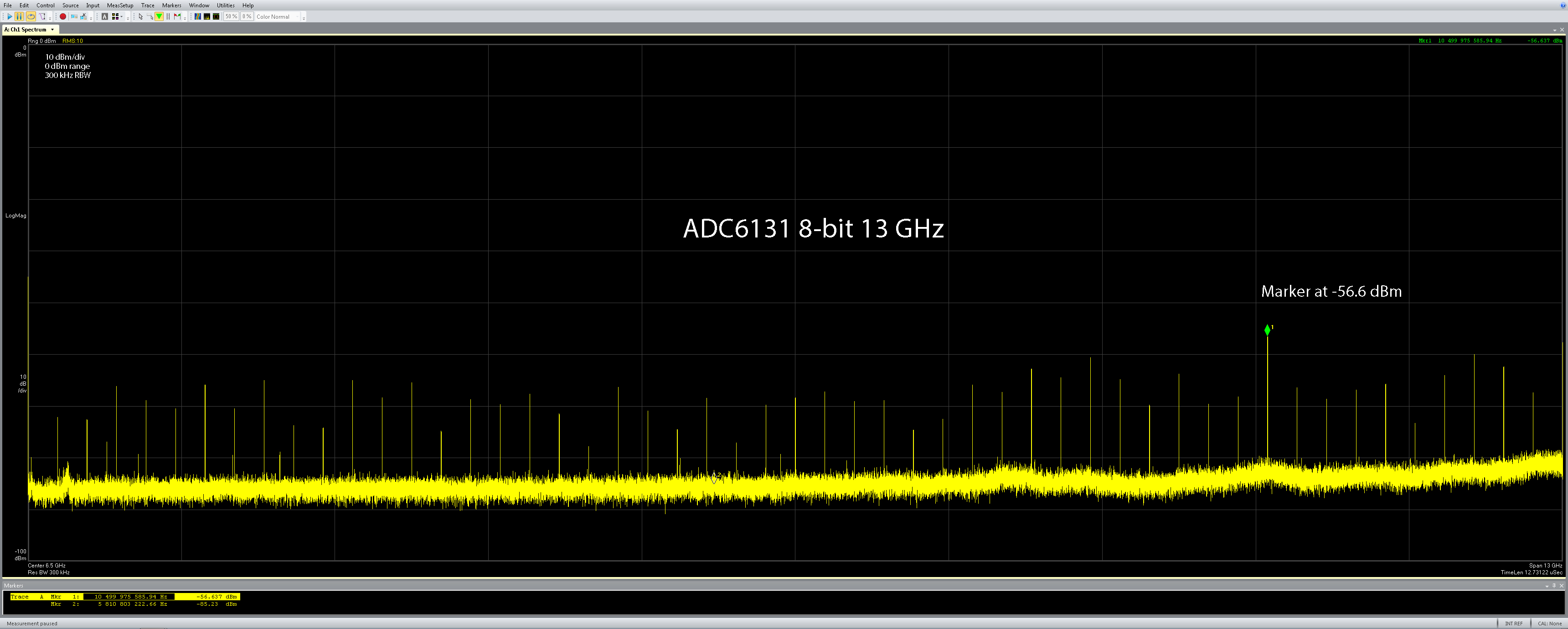
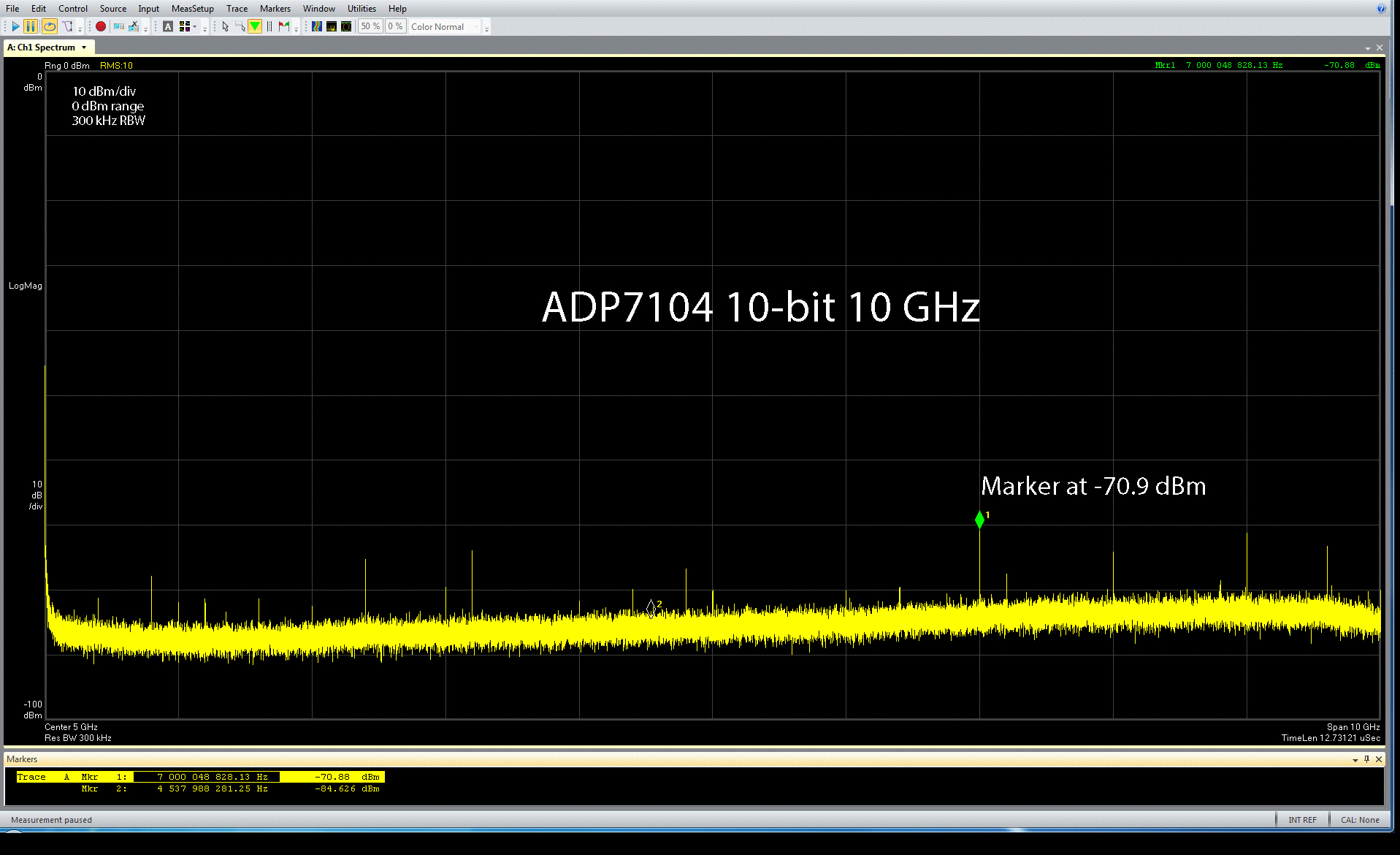
The ADP7000 digitizers have much improved noise floor and fewer spurious components compared to 8-bit technology.
- Using: 7,408,495 Digital equalization of multiple interleaved analog-to-digital converters – August 5, 2008
The digitizer has excellent internal ADC sample clock reference with low phase noise shown below:
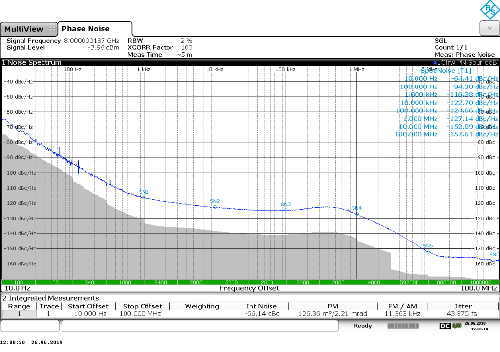
Note the phase noise above is measured with Rohde & Schwarz FSWP8 Phase Noise Analyzer and VCO Tester under static condition and excludes microphonic sensitivity.
RF Characteristics
For wideband RF applications, the preliminary RF characteristics for the ADP7104 Series Digitizer are listed below with graphs showing characterization results. Preliminary RF characteristics values from measured results with ADP7104 in 2-channel 32 Gsa/s mode.
| Measured with ADP7104 | ||
|
Sensitivity / Noise Density Power spectral density measurement at 1.0001 GHz |
-32 dBm range 1.0001 GHz center frequency 500 kHz span 3 kHz RBW |
-160 dBm/Hz |
| Signal-to-noise Ratio / Dynamic Range |
Derived from measurement above | 14 dB |
| Phase Noise – Carrier 1.4 GHz (M9505A chassis fans set to 60% speed) |
10 kHz offset | -128 dBc/Hz |
| 100 kHz offset | -132 dBc/Hz | |
| 1 MHz offset | -137 dBc/Hz | |
| 10 MHz offset | -141 dBc/Hz | |
| Phase Noise – Carrier 5.6 GHz (M9505A chassis fans set to 60% speed) |
10 kHz offset | -118 dBc/Hz |
| 100 kHz offset | -120 dBc/Hz | |
| 1 MHz offset | -129 dBc/Hz | |
| 10 MHz offset | -135 dBc/Hz | |
| EVM | 802.11 2.4 GHz carrier 20 MHz wide 64 QAM -3dB Full Scale |
-46 dB (0.5%) |
| 802.11 5.8 GHz carrier 20 MHz wide 64 QAM -4dB Full Scale |
-47 dB (0.47%) | |
| Two-tone Third-Order Intercept (TOI) Point – IMD3 |
0 dBm input tones 2.436 GHz and 2.438 GHz, 2 MHz separation 2.437 GHz center frequency 10 MHz span 30 kHz RBW 8 dBm input range |
+26.6 dBm |
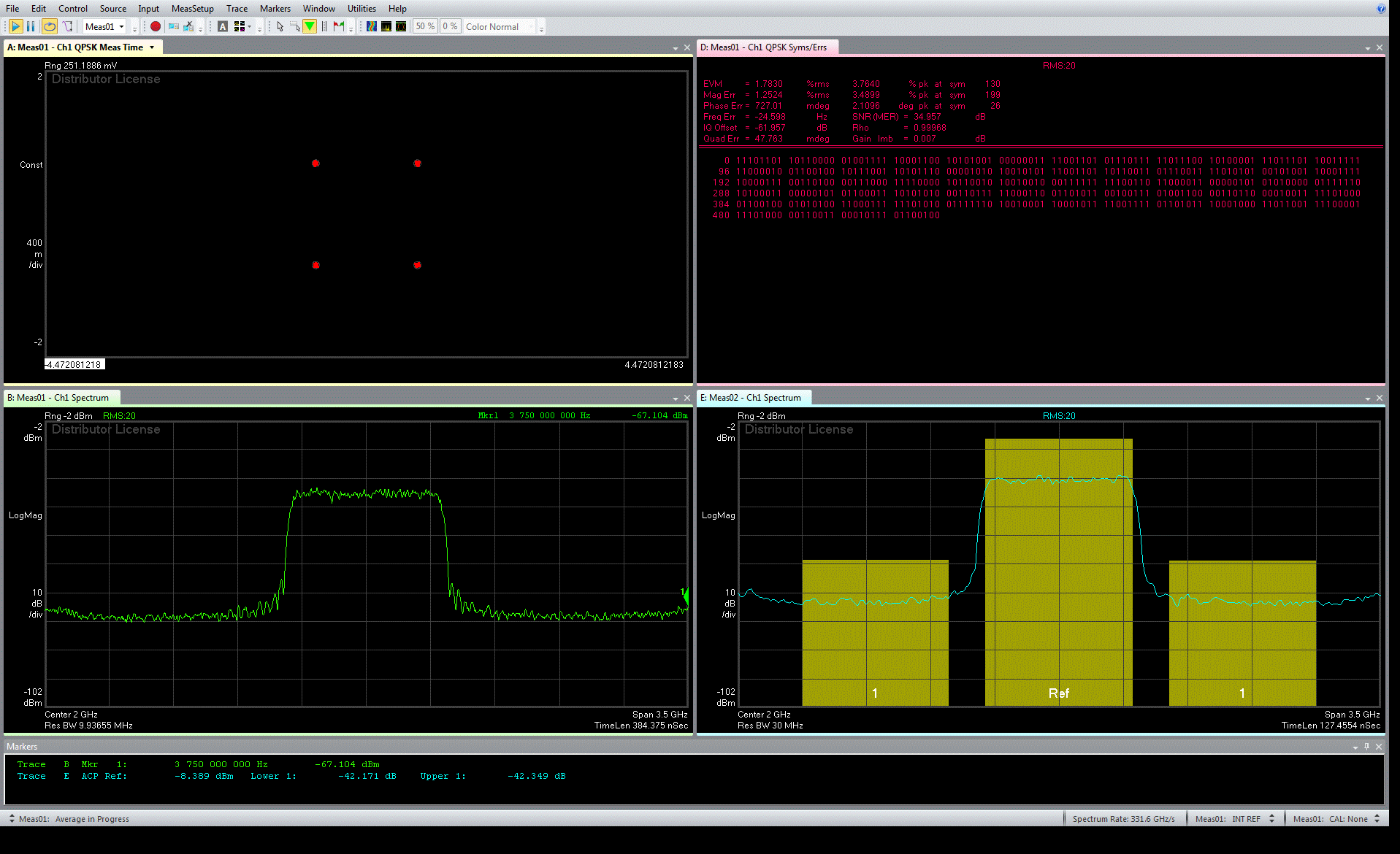
It is critical to have good Adjacent Channel Leakage Power Ratio (ACLR), also known as the Adjacent Channel Power Ratio (ACPR). It is defined as the ratio between the total power of the adjacent channel to the power of the carrier channel. Below is wide-band 2.4 GHz signal bandwidth 3×800 MHz QPSK with 1 GHz spacing at IF carrier (0.1 Alpha filter) generated by M8195A. Measured EVM and ACP-Adjacent Channel Power with VSA 89600 using ADP7104
| IF | EVM% | EVM% with Adaptive EQ | ACP Lower dB | ACP Ref dBm | ACP Upper dB |
| 2 GHz | 1.783 | 1.0663 | -42.171 | -8.389 | -42.349 |
| 2.5 GHz | 1.7817 | 1.0422 | -41.226 | -8.63 | -42.015 |
| 3.5 GHz | 1.7787 | 1.1182 | -41.277 | -8.836 | -41.039 |
| 4.5 GHz | 1.4337 | 1.1605 | -41.295 | -8.81 | -40.496 |
| 5.5 GHz | 1.553 | 1.2382 | -40.603 | -8.975 | -39.853 |
| 6.5 GHz | 2.0493 | 1.4816 | -39.249 | -9.034 | -38.864 |
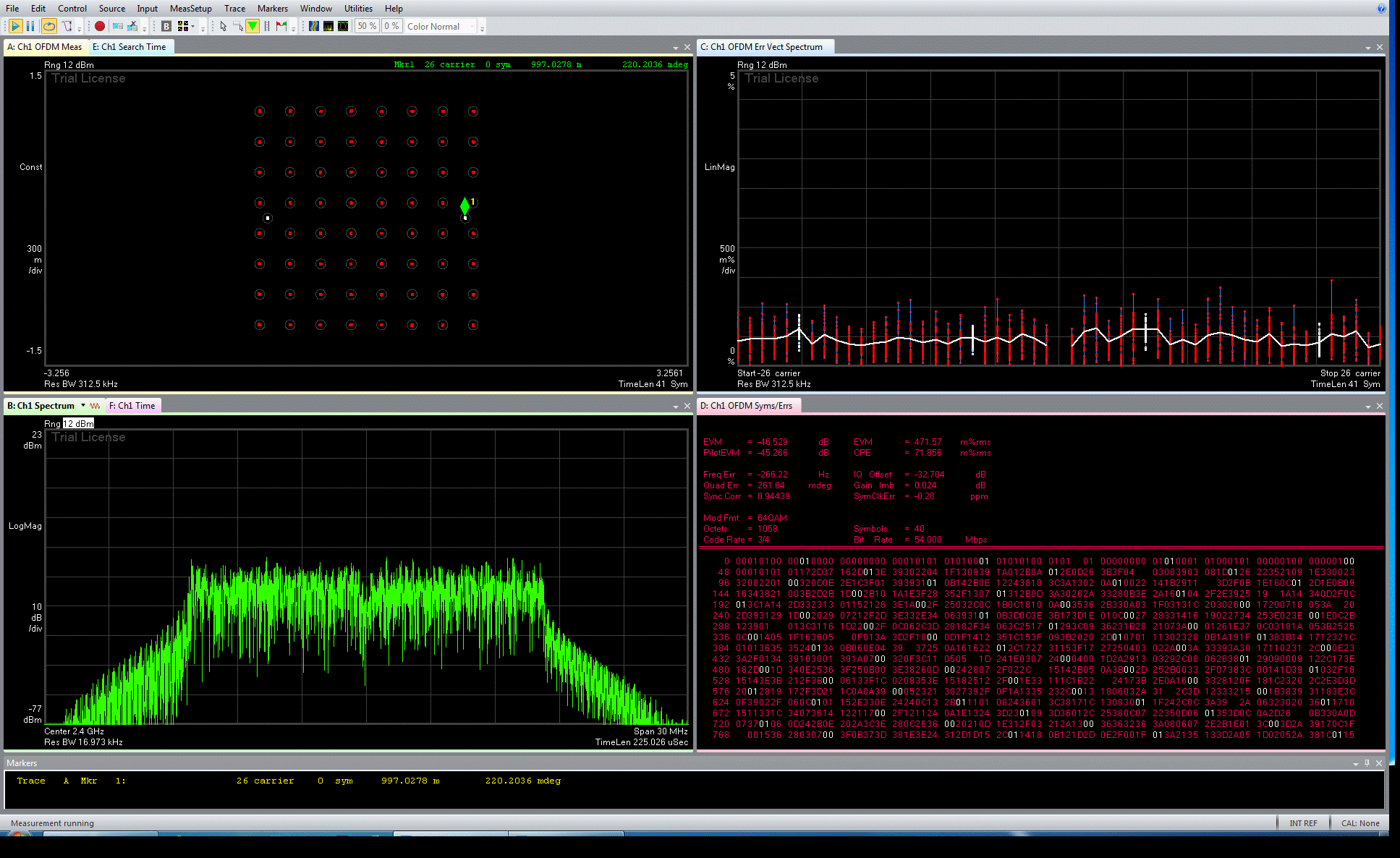
VSA shows an EVM for IEEE 802.11 QAM 64 centered at 2.4 GHz of 0.5%. Modulated signal generated by N5182B MXG X-Series RF Vector Signal Generator with Internal Correction Factors turned On.

VSA shows an EVM for IEEE 802.11 QAM 64 centered at 5.8 GHz of 0.47%. Modulated signal generated by N5182B MXG X-Series RF Vector Signal Generator with Internal Correction Factors turned On.
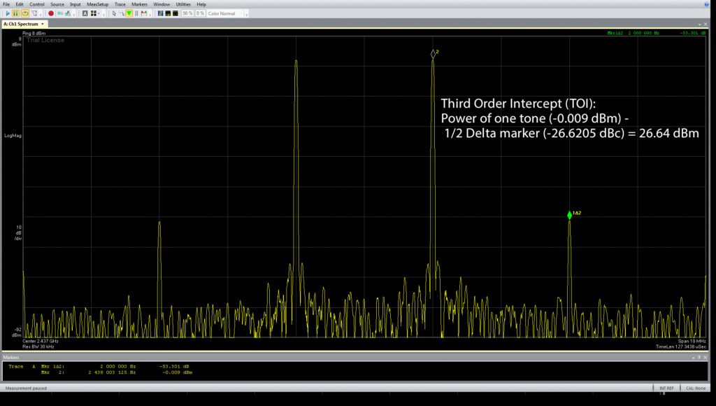
VSA shows an excellent TOI value of 26.6 dBm. Signals generated by two phase locked Keysight 83712B Synthesized CW Generators, combined through coax low-pass filters, attenuators and Keysight 11667B Power Splitter.
Specifications[4]
| Vertical System ADP7000 | ADP7084 | ADP7104 | ||||
| 2 Channel Mode – 20 Gsa/s |
2 Channel Mode – 20 Gsa/s |
4 Channel Mode – 10 Gsa/s |
2 Channel Mode – 32 Gsa/s |
2 Channel Mode – 32 Gsa/s |
4 Channel Mode – 16 Gsa/s |
|
| Input Channels | 2, SMA Female |
2, SMA Female |
4, SMA Female |
2, SMA Female |
2, SMA Female |
4, SMA Female |
| Analog Bandwidth (-3dB) [1],[2] | 8 GHz | 4 GHz | 4 GHz | 10 GHz | 6.5 GHz | 6.5 GHz |
| Bandwidth Flatness[1] (-6 dBFs) |
± 0.5 dB to 7.5 GHz |
± 0.5 dB to 3.5 GHz |
± 0.5 dB to 3.5 GHz |
± 0.5 dB to 8.5 GHz |
± 0.5 dB to 5 GHz |
± 0.5 dB to 5 GHz |
| -3 dB @ 8 GHz |
-3 dB @ 4 GHz |
-3 dB @ 4 GHz |
-3 dB @ 10 GHz |
-3 dB @ 6.5 GHz |
-3 dB @ 6.5 GHz |
|
| Vertical Resolution | 10 bits | |||||
| Input Impedance | 50 Ohm ± 3.5% (typical ± 1% at 25 °C) |
|||||
| Input Coupling | DC | |||||
| Maximum Input Voltage | ± 5 V | |||||
| Input Sensitivity (calibrated) | 16 mV … 8 V (Full Scale) -32 dBm … +22 dBm with 1 dB steps (Full Scale Range) |
|||||
| Hardware bandwidth limit filters (user-selectable) |
20 MHz, 250 MHz, 1.4 GHz, 3.1 GHz (4 GHz/6.5 GHz alias filter for 10/16 Gsa/s operation) |
|||||
| Phase Response Deviation[1] (-3 dBFs, 400 mV Full Scale) Full Bandwidth |
± 2 deg | ± 1 deg | ± 1 deg | ± 2 deg | ± 1 deg | ± 1 deg |
| Effective Bits[1] (-3 dBFs, 400 mV Full Scale) Frequency 1 GHz |
6.5 | 7.0 | 6.7 | 6.2 | 6.6 | 6.5 |
| Rise / Fall Time [3] (10-90%) |
53.8 ps | 107.5 ps | 107.5 ps | 43 ps | 66.2 ps | 66.2 ps |
| Vertical System ADP7000 | ADP7084 | ADP7104 | |||||
|
Sensitivity (Full Scale) |
2 Channel Mode – 20 Gsa/s |
2 Channel Mode – 20 Gsa/s |
4 Channel Mode – 10 Gsa/s |
2 Channel Mode – 32 Gsa/s |
2 Channel Mode – 32 Gsa/s |
4 Channel Mode – 16 Gsa/s |
|
| RMS Noise Floor[1] | 16 mV | 291 uV | 170 uV | 172 uV | 375 uV | 233 uV | 236 uV |
| 40 mV | 307 uV | 182 uV | 192 uV | 384 uV | 245 uV | 254 uV | |
| 80 mV | 366 uV | 228 uV | 255 uV | 448 uV | 295 uV | 315 uV | |
| 160 mV | 527 uV | 348 uV | 413 uV | 553 uV | 366 uV | 396 uV | |
| 400 mV | 1.234 mV | 810 uV | 988 uV | 1.492 mV | 1.114 mV | 1.198 mV | |
| 800 mV | 2.632 mV | 1.678 mV | 2.016 mV | 3.07 mV | 2.347 mV | 2.437 mV | |
| 1.6 V | 5.348 mV | 3.418 mV | 4.078 mV | 5.9 mV | 4.689 mV | 4.94 mV | |
| 4 V | 12.425 mV | 8.332 mV | 10.127 mV | 13.802 mV | 10.658 mV | 11.266 mV | |
| 8 V | 21.807 mV | 14.809 mV | 18.696 mV | 23.279 mV | 17.347 mV | 20.149 mV | |
| Spurious Free Dynamic Range (SFDR)[1] (-3 dBFS, 400 mV Full Scale) Frequency 1 GHz Excluding in-band 2nd and 3rd harmonics |
66.6 dBc | 71.4 dBc | 67.3 dBc | 70.1 dBc | 66.6 dBc | 68.1 dBc | |
| Nonlinear Distortions 2nd and 3rd harmonics |
2 GHz | 59.7 dBc | 58.8 dBc | 58.7 dBc | 61 dBc | 61.1 dBc | 60.3 dBc |
| 3 GHz | 53.9 dBc | 53.8 dBc | 53.9 dBc | 52.6 dBc | 52.5 dBc | 51.8 dBc | |
| DC Gain Accuracy | ± 3% of full scale at full resolution (± 1% for 40 mV to 8 V Full Scale) |
||||||
| Offset Range All Sensitivities |
± 4.5 V | ||||||
| Offset Accuracy | TBD | ||||||
| Channel to Channel Isolation (any two channels with equal Vertical settings) |
100 MHz … 1 GHz |
72 dB | |||||
| > 1 GHz | 49 dB | ||||||
| Vertical System ADP7000 | ADP7084 | ADP7104 | |||||
|
Sensitivity (Full Scale) |
2 Channel Mode – 20 Gsa/s |
2 Channel Mode – 20 Gsa/s |
4 Channel Mode – 10 Gsa/s |
2 Channel Mode – 32 Gsa/s |
2 Channel Mode – 32 Gsa/s |
4 Channel Mode – 16 Gsa/s |
|
| Return Loss | < 320 mV 0 … 9 GHz |
16 dB | 16 dB | 16 dB | 16 dB | 16 dB | 16 dB |
| > 320 mV 0 … 9 GHz |
19 dB | 19 dB | 19 dB | 19 dB | 19 dB | 19 dB | |
| < 320 mV @ 10 GHz |
12 dB | 12 dB | 12 dB | 12 dB | 12 dB | 12 dB | |
| > 320 mV @ 10 GHz |
13 dB | 13 dB | 13 dB | 13 dB | 13 dB | 13 dB | |
| Acquisition System ADP7000 | ADP7084 | ADP7104 | |||||
| 2 Channel Mode |
2 Channel Mode |
4 Channel Mode |
2 Channel Mode |
2 Channel Mode |
4 Channel Mode |
||
| Maximum Real Time Sample Rate per Channel | 20 Gsa/s | 20 Gsa/s | 10 Gsa/s | 32 Gsa/s | 32 Gsa/s | 16 Gsa/s | |
| Maximum Memory Depth per Channel | 128 GBytes |
128 GBytes |
64 GBytes |
128 GBytes |
128 GBytes |
64 GBytes |
|
| Maximum Acquired Time per Channel at Highest Real Time Sample Rate | 5.2 seconds |
5.2 seconds |
5.2 seconds |
3.2 seconds |
3.2 seconds |
3.2 seconds |
|
| Trigger | |||||||
| Trigger Types | Internal digital edge trigger on an input channel | ||||||
| External edge gate input | |||||||
| Gate Input Gate In (1-4)Note: Inputs are resampled |
4, MCX Female | ||||||
| Impedance | 50 Ohm | ||||||
| Voltage Range | ± 2.5V | ||||||
| Trig. Level Range | ± 2.5V | ||||||
| Minimum pulse width |
5 ns | ||||||
| Threshold Resolution | 4 mV | ||||||
| Max. Frequency | 100 MHz | ||||||
| Hold-off time | 300 nanosecond in post-trigger mode (ADP7104) 350 nanosecond in pre-trigger mode (ADP7104) |
||||||
| Control Signal Connections | |||||||
| Sync Clock Input (Sync Clk In) |
1, MCX Female | ||||||
| Frequency | 1 GHz / 2 to 32 | ||||||
| Level | +2 to +10 dBm | ||||||
| Impedance | 50 Ohm | ||||||
| Coupling | AC | ||||||
| Slew Rate | >= 4V/ns | ||||||
| Lock range | +/- 2 ppm MAX | ||||||
| Sync Clock Output (Sync Clk Out) |
1, MCX Female | ||||||
| Frequency | ADP7084 125 MHz |
ADP7104 200 MHz |
|||||
| Level | 400 mV p/p nominal | ||||||
| Impedance | 50 Ohm | ||||||
| Coupling | AC | ||||||
| External 1 GHz Reference Input (1 GHz In) |
1, MCX Female | ||||||
| Level | 0 to +10 dBm | ||||||
| Impedance | 50 Ohm | ||||||
| Coupling | AC | ||||||
| Lock range | +/- 2 ppm MAX | ||||||
| 1 GHz Internal Reference Clock Oscillator Output (1 GHz Out) |
1, MCX Female | ||||||
| Level | 400 mV p/p nominal | ||||||
| Impedance | 50 Ohm | ||||||
| Coupling | AC | ||||||
|
Time base accuracy (TSA)
|
± 50 ppb (v. Temperature) + Aging | ||||||
| Aging = ± 2 ppm max/10 years max | |||||||
| Aging = ± 0.3 ppm/first year typical | |||||||
| Aging = ± 5 ppb/day typical | |||||||
| SSB Phase Noise | < -145 dBc/Hz (typical) at 10 kHz offset | ||||||
| Reference Clock Distributor Input (Sync Clk Distributor In) |
1, MCX Female | ||||||
| Impedance | 50 Ohm | ||||||
| Level Range | 0.4 – 3.0 V p/p | ||||||
| Coupling | AC | ||||||
| Reference Clock Distributor Outputs (Sync Clk Distributor Out 1-6) |
6, MCX Female | ||||||
| Impedance | 50 Ohm | ||||||
| Level Range | 0.4 V p/p nominal | ||||||
| Coupling | AC | ||||||
| Trigger Distributor Input (Trigger Distributor In) |
1, MCX Female | ||||||
| Impedance | 50 Ohm | ||||||
| Level Range | +/- 2.5 V | ||||||
| Coupling | DC | ||||||
| Trigger Distributor Outputs (Trigger Distributor Out 1-6) |
6, MCX Female | ||||||
| Impedance | 50 Ohm | ||||||
| Level Range | 0.4 V p/p nominal | ||||||
| Common Mode | 0 V | ||||||
| Coupling | DC | ||||||
| Test Outputs (Test Out 1 – 4) |
4, MCX Female | ||||||
| Level | 3.3V LV TTL | ||||||
| Calibrator Output (Cal Out) |
1, SMA Female | ||||||
| Impedance | 50 Ohm | ||||||
| Step Output (Step Out) |
1, SMA Female | ||||||
| Impedance | 50 Ohm | ||||||
| I/O External (IO Ext) |
Reserved | 1, Samtec ERF-8-020 | |||||
| External Modulation Input (Ext Mod In) |
Reserved | 1, MCX Female | |||||
| Spare | 1, MCX Female | ||||||
| Optical Data Interfaces (ODI 1 – 4) |
4, MTP/MPO 24 Fiber connector | ||||||
| Class I Laser | 850nm VCSEL | ||||||
| Optical Control Interfaces (ODI Ctrl) |
1, MTP/MPO 24 Fiber connector | ||||||
| Class I Laser | 850nm VCSEL | ||||||
| Host Computer | |
| Transfer Interface | One PCI-Express x4 Generation 3 connection |
| Transfer Speed from chassis to external PC | Up to 1.6 GByte/s via PCI-Express x8 Generation 2 link from PC to AXIe-1 Gen2 capable chassis. |
| Transfer Speed from module to chassis | Up to 1.6 GByte/s via PCI-Express x4 Generation 2 link to AXIe-1 module. |
| Operating System | 64-bit Windows 7 64-bit Windows 10 Linux/Windows Hybrid Configuration supported |
| Module Physical | |
| Form factor | 8U form factor 2-slot AXIe |
| Dimensions (WxHxD) | 2.36″ (60 mm) x 12.7″(322.5 mm) x 11.1″ (281.5 mm) |
| Weight | 11 lbs / 5 kg |
| Power | ADP7084 – 300 Watt Max |
| ADP7104 – 400 Watt Max | |
| Safety Standards (Recognition # E112967) |
IEC 61010-1:2010 / EN 61010-1:2010 |
| USA: ANSI/UL 61010-1:2012 | |
| Canada: CAN/CSA C22.2 No. 61010-1:2012 | |
| Safety of Class 1 Laser | IEC 60825-1:2007 / EN 60825-1:2007 (2nd Edition) Complies with 21 CFR 1040.10 and 1040.11 except for deviations pursuant to Laser Notice No. 50, dated June 24, 2007. |
| EMC Standards |
EN 61326-1:2013 Class A |
| CISPR 11:2009 / EN 55011:2009 + A1:2010 | |
| IEC 61000-4-2:2008 / EN 61000-4-2:2009 | |
| IEC 61000-4-3:2006 + A1:2007 + A2:2010 / EN 61000-4-3:2006 + A1:2008 + A2:2010 |
|
| IEC 61000-4-4:2004 + A1:2010 / EN 61000-4-4:2012 | |
| IEC 61000-4-5:2005 / EN 61000-4-5:2006 | |
| IEC 61000-4-6:2008 / EN 61000-4-6:2009 | |
| IEC 61000-4-11:2004 / EN 61000-4-11:2004 | |
| RoHS | EN 50581:2012 |
| Operating Temperature Range | +5 C to +40 C |
| Non-Operating Temperature | -40 C to +70 C |
| Operating humidity | 5% to 80% relative humidity, non-condensing |
| Operating Altitude | Up to 4,000 meters (12,000 feet) |
| Non-Operating Altitude | Up to 15,300 meters (50,000 feet) |
| Calibration interval | 1 year recommended |
________________
[1] With digital equalization
[2] 6-pole Butterworth approximation
[3] Calculated based on Tr = 0.43/BW
[4] Specification values provided are preliminary based on two samples. Specifications are subject to change.
| Hardware Base Modules: | P/N | Price | Typical Lead Time |
| MOD:ADP7084, 40GSa/sec ADC, 128 GByte AXIe Digitizer w/ “basic” software | S90-620200-02 | Call | In stock (Please call for lead time) |
| MOD:ADP7104, 64GSa/sec ADC, 128 GByte AXIe Digitizer w/ “basic” software | S90-620201-02 | Call | In stock (Please call for lead time) |
| DP7000, 128 GByte AXIe Digital Processor Module with “basic” software | S90-620202-02 | TBA | Call |
| Hardware Options: | |||
| UPGR:ADP7000 256 GByte Memory Hardware Upgrade | S95-990474 | Call | (Please call for lead time) |
| UPGR:ADP7000 Optics Upgrade for Control Hardware Upgrade | S95-990475 | Call | Available |
| UPGR:ADP7000 Optics Upgrade for Streaming Hardware Upgrade | S95-990467 | Call | Available |
| UPGR:ADP7084 to ADP7104 Hardware Upgrade | S95-990468 | Call | Available |
| WARR:EXTEND DIGITIZER HARDWARE WARRANTY FROM 1YRS TO 3YRS | S95-990661 | Call | Available |
| Firmware Options: | |||
| MSFT:ADC_BASE Equalization of Multiple Interleaved ADCs (1 YR SOFTWARE MAINTENANCE INCLUDED) | S87-777627 | Included with base module | |
| MSFT:ADC_SM Segmented Memory Acquisitions (1 YR SOFTWARE MAINTENANCE INCLUDED) | S87-777623 | Call | Available |
| MSFT:ADC_BB Baseband Filtering (1 YR SOFTWARE MAINTENANCE INCLUDED) | S87-777624 | Call | Available |
| MSFT:ADC_AVGA Real-Time Averaging (1 YR SOFTWARE MAINTENANCE INCLUDED) | S87‐777648 | Call | Available |
| MSFT:ADC_AVG High Speed Deep Averaging (1 YR SOFTWARE MAINTENANCE INCLUDED) | S87-777618 | Call | Available |
| MSFT:ADC_AVGS High Speed Deep Segmented Averaging (1 YR SOFTWARE MAINTENANCE INCLUDED) (Includes ADC_SM and ADC_AVG) |
S87-777625 | Call | Available |
| MSFT:ADC_AVGA Real-Time Asynchronous Averaging (1 YR SOFTWARE MAINTENANCE INCLUDED) | S87-777648 | Call | Q3 2019 |
| MSFT:ADC_ADDCRT1 Real-time Digital Down Converting (1 YR SOFTWARE MAINTENANCE INCLUDED) | S87-777644 | Call | Available |
| MSFT:ADC_VSM1 Real-time variable segment option, requires ADC_ADDCRT1 option (1 YR SOFTWARE MAINTENANCE INCLUDED) | S87-777642 | Call | Q3 2019 |
| MSFT:ADC_CEQRE1 Fast Complex Equalizer/Resampler using one GPU (1 YR SOFTWARE MAINTENANCE INCLUDED) | S87-777645 | Call | Available |
| MSFT:ADC_FFT1 Fast FFT with one GPU (1 YR SOFTWARE MAINTENANCE INCLUDED) | S87-777630 | Call | Available |
| MSFT:ADC_SYNC1 Multi-module synchronization capability (1 YR SOFTWARE MAINTENANCE INCLUDED) | S87-777639 | Call | Available |
| Accessories: | |||
| 4 x 36″ SMA-SMA coax input channel reference cables | S30-110789 | Included | Available |
| 1 x 60″ BNC-MCX coax external reference clock cable | S30-460488 | Included | Available |
| 1 x SMA torque wrench (8 in/lbs) | S59-109352 | Included | Available |
| Guzik Optical Bridge to PC PCIe host card 24F 14.1G |
S60-707115 | Call | Q3 2019 |
| Software Packages | |||
|
“Basic” software package includes:
|
|||


