Real-Time Signal Averaging
with External Trigger
Key Features
- 99% trigger efficiency
- Near zero overhead
- 20 microsecond segments (ADP7104 digitizer)
- Significantly faster than traditional averaging
Introduction
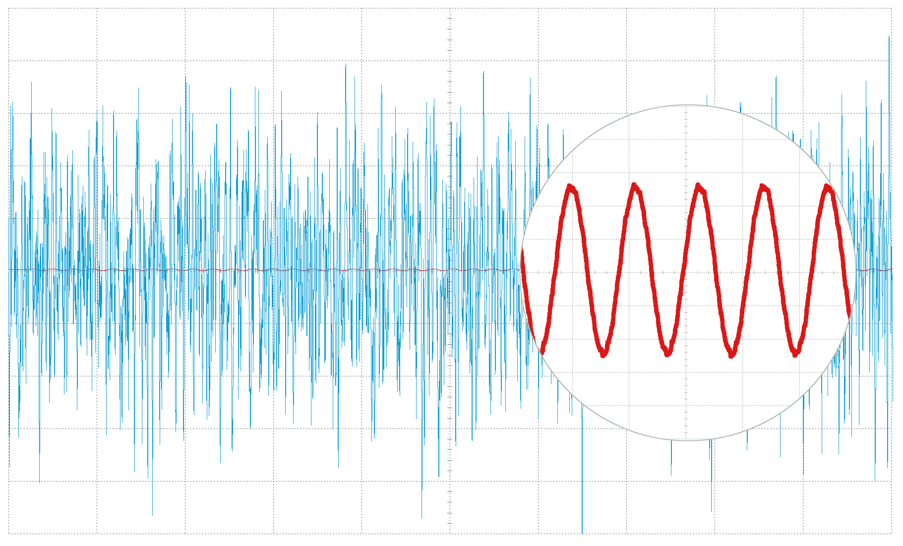
Signal averaging is commonly applied to improve the signal-to-noise ratio and detect small signals otherwise buried in noise. It is widely used in a variety of applications ranging from scientific research to high-speed communications.
The principles behind signal averaging are well known. Given repetitive signal S(t) and uncorrelated additive noise n(t), summation of N repetitive periods of the signal results in noise reduction. The signal amplitude increases linearly with the number of summations, however the noise adds as the power and the RMS noise amplitude increases as . Therefore, after N averages, the average signal equals to:
The signal-to-noise ratio improvement gain is proportional to . For example, the average of 100 signal periods provides the SNR gain of 10 times, or 20 dB; after 1 million averages the SNR is improved by 1,000 times, or 60 dB.
Impact of Trigger Jitter
Signal averaging should be performed relative to the precise timing signal (trigger), indicating the repetition of a signal period. If the trigger position is not stable, the signal will be distorted or worse completely averaged out. Therefore, the accuracy of the trigger which provides the exact position of the repetitive signal period is essential for the quality of the averaged signal.
To estimate how trigger jitter affects the quality of the averaged signal, the case of random waveform timing displacements , the average signal can be written as:
The Fourier transform of the average signal corresponds to the sum of random phase signals. For the normally distributed random displacements this spectrum can be represented as a Gaussian-shaped frequency response:
Where is the standard deviation of normally distributed random displacements
, or, in another words, trigger jitter RMS.
Trigger jitter may have dramatic impact on averaged waveforms. This is illustrated by Figure 1, showing the amplitude roll-off of the averaged signal magnitude as a function of the normalized signal frequency for different values of trigger jitter. When the trigger jitter RMS value equals to the ADC sampling period T, the amplitude at 70% of the Nyquist frequency is attenuated by more than 20 dB. Reducing jitter to 0.5T results in 5 dB attenuation. Clearly, trigger jitter should be as small as possible to avoid the amplitude distortion (attenuation) of the averaged signal at high frequencies.
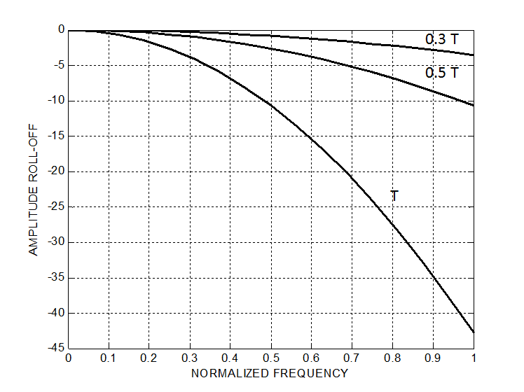
Figure 1. Amplitude roll-off of averaged signal for different trigger jitter values
Figure 2 demonstrates the averaging process of a sequence of linear frequency modulated (LFM) chirp pulses sampled at 32 GSa/s. Each signal period is a frequency sweep signal with the sweep frequency ranging from 1 to 10 GHz.
In the case of ideal trigger positions (the top row), the average signal is not distorted. When the RMS of the trigger jitter equals 10 ps (the bottom row) each period of the waveform will not be exactly aligned in the time domain. Resulting signal distortions are stronger at higher frequencies, since the displacement of each individual waveform corresponds to a higher fraction of the high frequency signal period. The averaging result demonstrates strong frequency-dependent roll-off and the distorted shape of the LFM chirps.
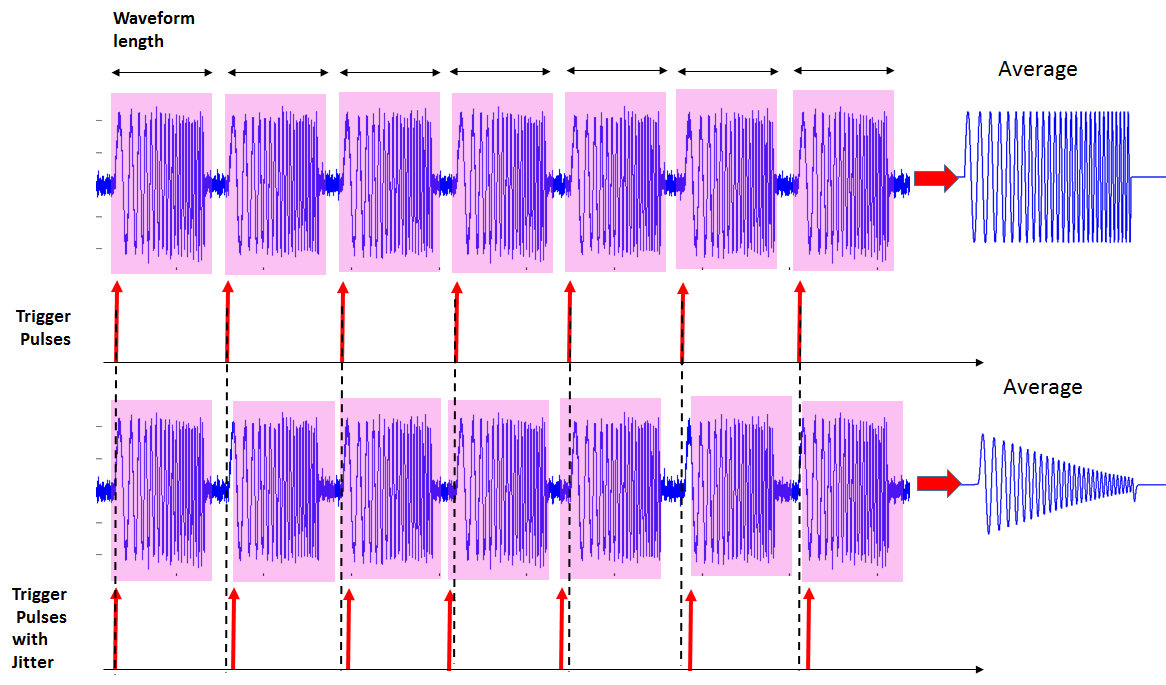
Figure 2. LFM chirp after averaging with and without trigger jitter
Impact of Sub-sample Alignment
Low trigger jitter is not sufficient for distortion-free signal averaging. When the trigger is detected within the ADC sampling interval, the acquisition starting point is still limited by the ADC sampling clock period. The trigger position may occur anywhere inside the ADC sampling period (see Figure 3).
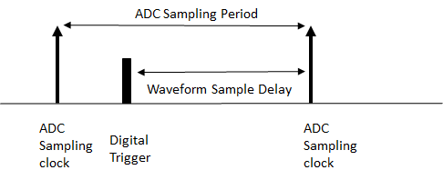
Figure 3. Trigger position in respect to the ADC sampling clock
A typical implementation of averaging uses the straight-forward approach in which the digitized waveforms acquired at different trigger events are simply summed together sample-by-sample. The first sample in each waveform is selected as the closest to the trigger event time point.
The following estimates how the simple sample averaging approach affects the averaged signal quality.
When the trigger position is independent of the ADC sampling clock, the distribution of trigger locations inside the ADC sampling intervals is approximately uniform within the sampling interval. The Fourier transform of the uniform distribution (characteristic function) has the frequency response given by the following formula:
This frequency response is shown in Figure 4 for the signal frequency normalized to Nyquist frequency.
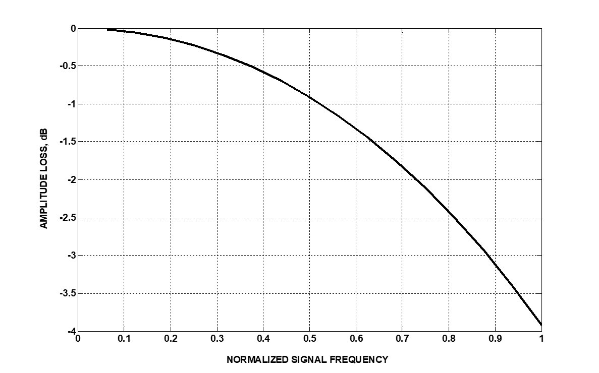
Figure 4. Amplitude roll-off of averaged signal in case of sample averaging
For example, for 16 GSa/s sampling rate and 6.5 GHz analog bandwidth (which corresponds to 6.5 GHz / (0.5 * 16 GSa/s) = 0.81 normalized frequency), the signal averaged by sample averaging approach will be attenuated by about 2.5 dB.
To reduce frequency roll-off, sub-sampling averaging is performed1. Four sub-sample average intervals reduce high frequency attenuation to about 0.13 dB.
For 32 GSa/s sampling rate and 10 GHz analog bandwidth (normalized frequency of 0.625), sub-sample average intervals reduce attenuation to about 0.3 dB.
Averaging Limitations in Digital Oscilloscopes
Waveform averaging is a standard feature of modern digital oscilloscopes. However, oscilloscope-based averaging has a number of limitations:
- Low averaging speed and trigger efficiency. Typically, the averaging operation is slow since system resources are spent on memory transfer and waveform display. This causes low trigger utilization rates as most of signal periods are missed. Many applications require tens of millions of averages for signal detection, which takes hours or even days using oscilloscopes.
- Small length of averaged waveform. Typically, a waveform length is limited by available system memory. Some oscilloscopes allow averaging of longer waveforms in their memory. However, the speed of averaging is dramatically reduced compared to the maximum available one (real time) due to read-accumulate-store memory operation required for each waveform.
- Triggering accuracy. Since the resulting average is a convolution of the jitter probability density distribution function (PDF) and the underlying waveform, the greater trigger jitter (or trigger uncertainty) results in the more distorted averaged waveforms.
- ADC sampling rate limitation. Most digital oscilloscopes use sample averaging of digitized signal, therefore any improvements in trigger event detection are limited by the ADC sampling rate.
Real-Time Signal Averaging Option for Guzik ADP7000 and VR8042 Digitizers

Figure 5. ADP7000 and VR8042 digitizers
For Guzik ADP7000 and VR8042 digitizers (see Figure 5), Guzik Technical Enterprises offers the real-time signal averaging option, which addresses all the limitations discussed in the previous sections.
To overcome the trigger jitter limitation, Guzik digitizers incorporate a dedicated low-jitter external trigger with advanced digital signal processing2. The external trigger converts an analog trigger pulse to a very high accuracy digital timing position. The typical jitter of the external trigger is below 1 ps RMS.
To address the ADC sampling rate limitation, Guzik digitizers use a patented real-time oversampling averaging method. This approach provides sub-sample accuracy of the signal alignment without the computation-intensive signal resampling. This allows real-time implementation with the on-board FPGA (Field Programmable Gate Array) devices.
The real-time averaging, performed by the digitizer’s on-board FPGA, addresses the problems of low averaging speed and trigger efficiency. Since the data accumulation is performed in real-time (on the fly), there are very few missed trigger events. In a typical scenario, trigger utilization is more than 99%.
The pipelined design of FPGA processing is optimized to reduce the dead time between segments: the time needed to rearm the acquisition of the next segment after the completion of the previous segment (see Figure 6) and be ready to accept the next segment. For ADP7000, the rearm time is 25 ns. Combined with the minimum segment duration of 15 ns, this yields the maximum trigger rate of 25 MHz: 15 ns minimum segment time plus 25 ns rearm time gives 40 ns minimum trigger period, which is 25 MHz.
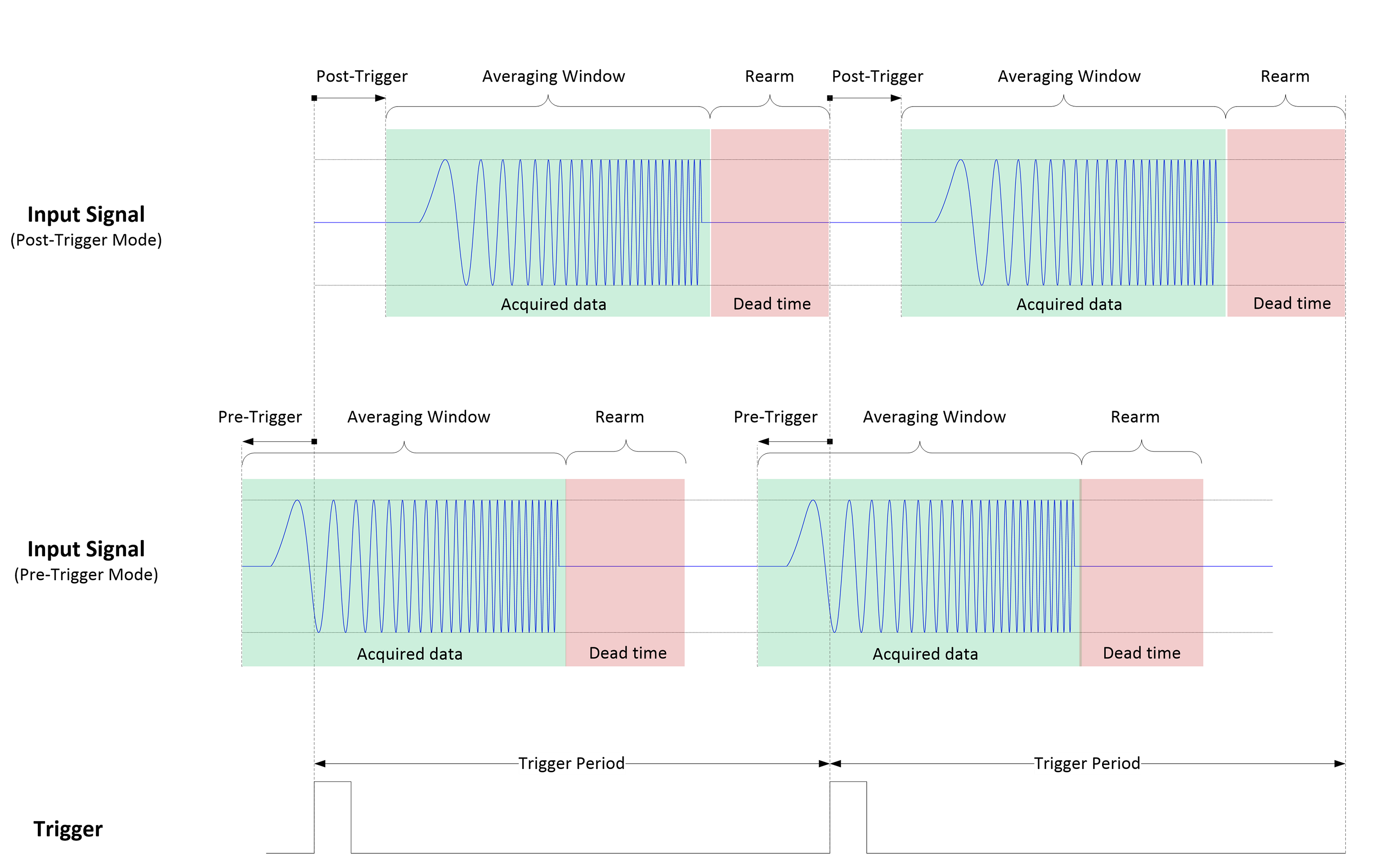
Figure 6. Segmented acquisition timing diagram
Also, to provide more flexibility in measurement scenarios, both pre-trigger delay and post pre-trigger delay are supported (see Figure 6). This allows to move the triggering time point in both directions with respect to the signal to be averaged.
An example of a signal detection heavily buried in noise using real-time averaging is shown in Figure 7. The source signal is mixed with additive noise from the noise generator and has an SNR of ‑36 dB. This means that the signal power is 4,000 times lower than the power of noise. The progression of averaging is demonstrated as a sequence of averaged waveforms with ten-fold average count increase from a waveform to a waveform.
After 100,000 averages the signal becomes visible with the SNR of approximately 14 dB. After 10,000,000 averages, the presence of noise is further reduced, and the signal can be seen with an SNR of about 34 dB. With Guzik real-time averaging, 10 million averages were performed in 5 seconds using 2 MHz trigger repetition rate, delivering 99% trigger utilization.
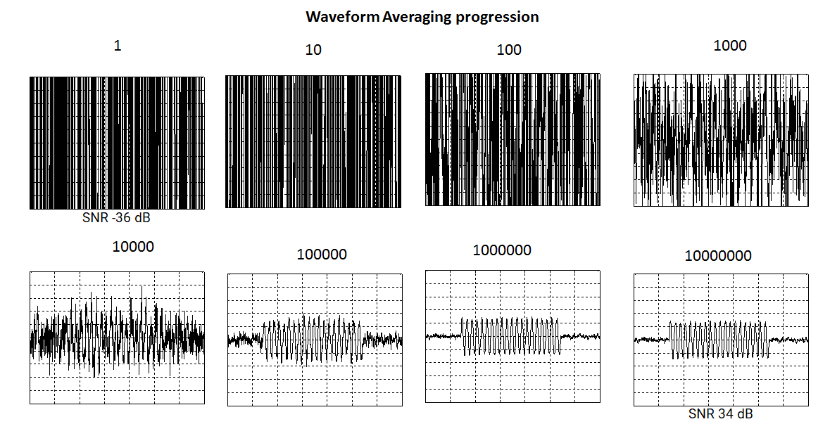
Figure 7. Real-time signal averaging at -36 dB SNR, showing progression of 10 million averages completed in 5 s
Classifying Marker
For even greater flexibility, real-time averaging has the classifying marker mode of operation. In certain applications, it is required to differentiate averaged waveform depending on additional external classifying signal. In the very basic scenario one may want to average and then compare waveforms with a “good” qualifier against waveforms with a “bad” qualifier. This qualifier is supplied by external circuitry once per each of analyzed (averaged) waveforms.
This mode requires that a third signal be supplied to the digitizer: the classifying marker signal. This signal must be connected to an external gate channel labeled GATE IN. The level and slope (rising or falling) for the classifying marker are specified similar to those for triggers. In addition, the channel used to supply the classifying marker signal should be specified, and, finally, the classifying marker interpretation mode. These descriptions define a classifying event, the presence of which is analyzed by the processing. A classifying event is said to be present for a particular segment if an edge transition matching the user-specified classifying parameters occurs between the main trigger event corresponding to said segment, and the next main trigger event.
There are four classifying event interpretation modes:
- Off
- Accept
- Reject
- Classify
Off mode ignores the classifying events – all segments are averaged into one common bucket.
In Accept mode, averaging of a particular segment only occurs if a classifying event is detected.
In Reject mode, averaging of a particular segment only occurs if a classifying event is not detected.
The Classify mode separately averages segments based on classifying event detection (or non-detection) into different averaging buckets. The absence of the classifying event results in averaging into averaging bucket #0, and the presence of the classifying event results in averaging into averaging bucket #1. In ADP7104, eight averaging buckets are supported when three GATE IN inputs are used. The VR8042 supports two averaging buckets with one GATE IN signal.
Figure 8 shows the timing diagram of single-bit classifying marker operation in Classify mode:
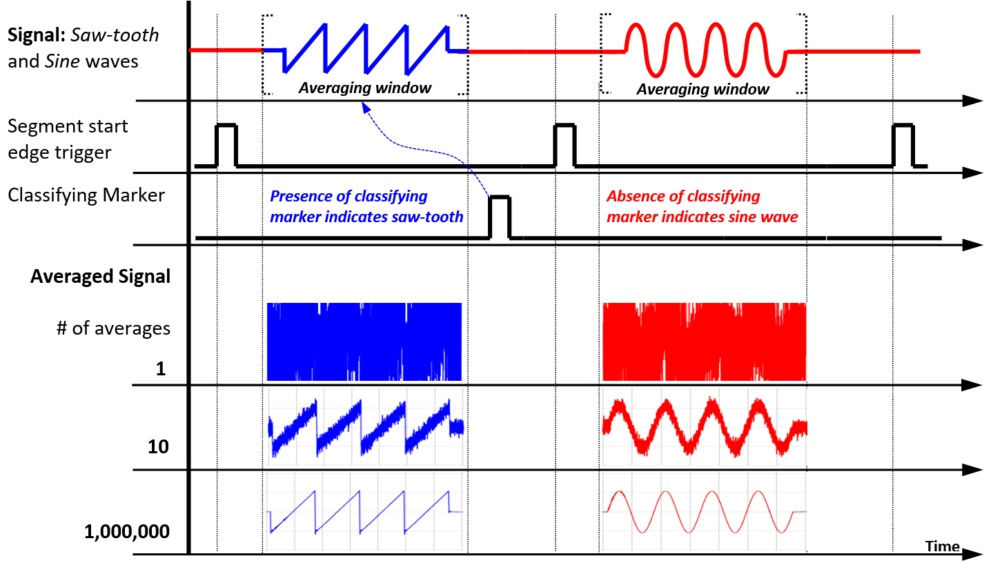
Figure 8. Classifying marker timing diagram
The input signal consists of two types of segments. The first type of segments (blue color) contains the saw-tooth signal. The classifying marker pulse is present within this type of segments. The second type of segments (red color) contains the sine-wave signal. The classifying marker pulse is absent within this type of segments. The Classify mode averages the saw-tooth segments into one averaging bucket, and the sine-wave segments into another averaging bucket, allowing automatic separation of different types of signals into different averaging buckets.
Real-Time Averaging with Decimation
Real-time averaging with decimation can be used to extend the averaging window length proportional to the decimation factor while further improving SNR and ENOB. Decimation factor ranges from 2 to 64. The VR8042 digitizer at maximum decimation of 64 extends the averaging window to 832 microseconds per channel.
Specification3
ADP7104 Digitizer
| Input sensitivity (full scale) | 16 mVpp … 8 Vpp (-32 dBm … +22 dBm with 1 dBm step | |
| Averaged waveform sample width | 64-bit floating point | |
| ADC sampling rate (resolution) | 32 GSa/s (10-bit) | 16 GSa/s (10-bit) |
| Analog bandwidth | 10 GHz | 6.5 GHz |
| Number of channels | 2 | 4 |
| Number of averages | > 50 million (with 256 GB memory option) | |
| Averaging window | Min: 15 ns Max: 20 µs (640,000 points @ 32 GSa/s, single segment) 10/5/2.5 µs for 2/4/8 conditions of classifying marker |
|
| Averaging time (500 ns trigger period and 107 averages performed) |
5.7 s (5 s signal time) | |
| Trigger: RMS jitter | ≤ 0.8 ps | |
| Maximum trigger rate | 25 MHz | |
| Rearm time4 | 25 ns | |
| Trigger utilization | ≥ 99% | |
| Pre-trigger range | 0 … 4.5 µs in 5 ns increments | |
| Post-trigger range | 0 … 21 s in 5 ns increments | |
| Classifying marker: Number of conditions | up to 8 | |
| Proximity to trigger | > 20 ns separation between trigger and classifying marker edges | |
| Adjustment to trigger | -4.0 µs to 0.25 µs in 5 ns increments | |
| Trigger-to-data alignment accuracy | better than 10 ps | |
| Data transfer speed from digitizer | Up to 1.5 GByte/s (via PCIe Gen2 x4 link) Up to 10 Gbyte/s (with optional optical link) | |
VR8042 Digitizer
| Input sensitivity (full scale) | 64 mVpp … 8 Vpp (-20 dBm … +22 dBm with 1 dBm step) |
| Averaged waveform sample width | 64-bit floating point |
| ADC sampling rate (resolution) | 10 GSa/s (12-bit) |
| Analog bandwidth | 4 GHz |
| Bandwidth flatness | < ±0.2 dB to 3.6 GHz |
| Rise / fall time (10 – 90%) | 110 ps |
| Phase response to 4 GHz | ±1.5 deg |
| Number of channels | 2 |
| Number of averages (per channel with max averaging window of 13 µs) |
67 million |
| Averaging window | Min: 12.8 ns Max: 13 µs 6.5 µs for 2 conditions of classifying marker |
| Averaging time (10 µs trigger period and 107 averages performed) |
100.7 s (100 s signal time) |
| Trigger: RMS jitter | ≤ 1 ps |
| Maximum trigger rate | 30 MHz |
| Rearm time | 12.8 ns |
| Trigger utilization | ≥ 99% |
| Pre-trigger range | 0 … 6.08 µs in 6.4 ns increments |
| Post-trigger range | 0 … 27.488 s in 6.4 ns increments |
| Classifying marker: number of conditions | 2 |
| Proximity to trigger | > 6.4 ns separation between trigger and classifying marker edges |
| Adjustment to trigger | -13 µs to 0.025 µs in 6.4 ns increments |
| Trigger-to-data alignment accuracy | better than 5 ps |
| Data transfer speed from digitizer | Up to 10 GByte/s |
Real-Time Averaging with Decimation
| Decimation Factor | Sampling Rate (GSa/s) | Analog Bandwidth (GHz) | Averaging Window (µs) | Rearm Time (ns) |
| 1 | 10 | 4 | 13 | 12.8 |
| 2 | 5 | 2 | 26 | 25.6 |
| 4 | 2.5 | 1 | 52 | 51.2 |
| 8 | 1.25 | 0.5 | 104 | 102.4 |
| 16 | 0.625 | 0.25 | 208 | 204.8 |
| 32 | 0.3125 | 0.125 | 416 | 409.6 |
| 64 | 0.015625 | 0.0625 | 832 | 819.2 |
1 US Patent 10,848,168
2 US Patent 10,924,130
3 Specifications are subject to change without notice
4 The trigger rearm time indicates the time interval when the digitizer cannot detect triggers after the acquisition completion

